-

Mitsubishi Electric Corporation announced that it will enter into a strategic partnership with Nexperia B.V. to jointly develop silicon carbide (SiC) power semiconductors for the power electronics market. Mitsubishi Electric will leverage its wide-bandgap semiconductor technologies to develop and supply SiC MOSFET chips that Nexperia will use to develop SiC discrete devices.
The electric vehicle market is expanding worldwide and is helping to drive the exponential growth of SiC power semiconductors, which offer lower energy loss, higher operating temperatures and faster switching speeds than conventional silicon power semiconductors. The high efficiency of SiC power semiconductors is expected to contribute significantly to global decarbonization and green transformation.
Mitsubishi Electric has established leading positions in applications such as high-speed trains, high-voltage industrial applications and home appliances. The company launched the world’s first SiC power modules for air conditioners in 2010 and became the first supplier of an all-SiC power module for Shinkansen bullet trains in 2015. Mitsubishi Electric has accumulated superior expertise for the development and manufacture of SiC power modules, which are known for their advanced performance and high reliability.
Going forward, Mitsubishi Electric expects to strengthen its partnership with Nexperia, a global leader with decades of experience in the design, manufacture, quality assurance and supply of diverse discrete devices. Nexperia’s devices are used in the automotive, industrial, mobile and consumer markets, contributing to decarbonization and a more sustainable future. Mitsubishi Electric will continue to improve the performance and quality of its SiC chips and focus on the development of power modules using proprietary module technologies.
Mark Roeloffzen, SVP & General Manager Business Group Bipolar Discretes at Nexperia, said: “This mutually beneficial strategic partnership with Mitsubishi Electric represents a significant stride in Nexperia’s silicon carbide journey. Mitsubishi Electric has a strong track record as a supplier of technically proven SiC device and modules. Combined with Nexperia’s high-quality standards and expertise in discrete products and packaging, we will certainly generate positive synergies between both companies – ultimately enabling our customers to deliver highly energy efficient products in the industrial, automotive or consumer markets they serve.”
Masayoshi Takemi, Executive Officer and Group President, Semiconductor & Device at Mitsubishi Electric, said: “Nexperia is a leading company in the industrial sector with proven technologies for high quality discrete semiconductors. We are delighted to enter into this co-development partnership that will leverage the semiconductor technologies of both companies.”
Original – Mitsubishi Electric
-
ROHM has completed the acquisition of the assets of Solar Frontier’s former Kunitomi Plant located in Japan, on November 7, 2023, based on its basic agreement signed with Solar Frontier.
The Plant will be operated by LAPIS Semiconductor, a subsidiary of the ROHM Group, as its Miyazaki Plant No.2. It will become the Group’s main production site for SiC power devices and is aiming to start operation during 2024.
The ROHM Group will continue to strengthen its production capacity in accordance with its Medium-Term Management Plan while keeping abreast of market conditions, and will also thoroughly enhance its BCM system to ensure a stable supply of products to customers.
Original – ROHM
-
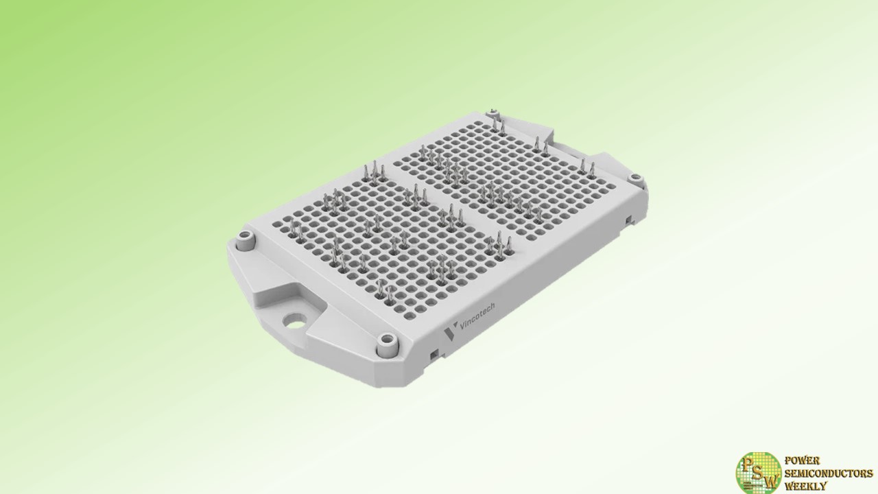
Engineered for maximum power density, this half-bridge module can serve to construct excellent H-bridges and sixpacks. Far higher current handling, enhanced power loss dissipation, greater scalability than a solution with a single-module footprint – the flowDUAL delivers all this and more.
In combination with VINcoPress and advanced die-attach technology, this new baseplate-less module from Vincotech is your first choice for a wide range of high-power use cases where utmost efficiency and reliability are top priorities.
Main benefits
- Outstanding, ≥99% conversion efficiency brings down overall costs
- Low stray inductance and symmetrical chip layout enable higher switching frequency and lower system costs
- Greater supply chain security with
– the new flow E3 industry standard-compatible housing (CTI >600)
– the latest multi-sourced SiC devices - Excellent thermal performance with VINcoPress technology to decrease junction temperature and increase lifetime
- Pre-applied PC-TIM rated for 150°C helps reduce production cost
Applications
- Industrial drives
- Embedded drives
- EV Chargers
- Solar
- UPS
Original – Vincotech
-
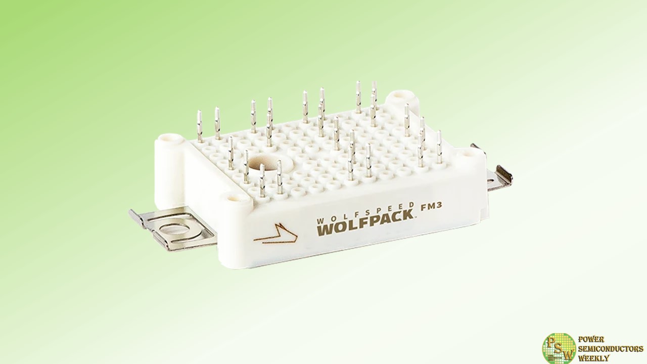
The Wolfspeed WolfPACK power module family is designed to give engineers choice and flexibility when working on power electronics applications greater than 10 kW.
In addition to half-bridge and six-pack topologies, WolfPACK modules are now available in full-bridge configurations—all with the option for pre-applied Honeywell™ PTM6000 Series TIM.
Selecting pre-applied TIM can reduce assembly cost and complexity, while improving reliability and performance. Compared to standard grease solutions, WolfPACK modules with pre-applied TIM can reduce the junction temperature by 40°C under the same conditions or increase current capability by 60% due to the reduction in thermal resistance.
All WolfPACK modules are designed to provide clean, reliable power for energy conversion systems. By leveraging more than 35 years of vertically integrated industry experience, Wolfspeed ensures that these modules offer low losses in a package that lends itself to fast design implementation, scalability, long term design support, and lower assembly overhead.
Original – Wolfspeed
-
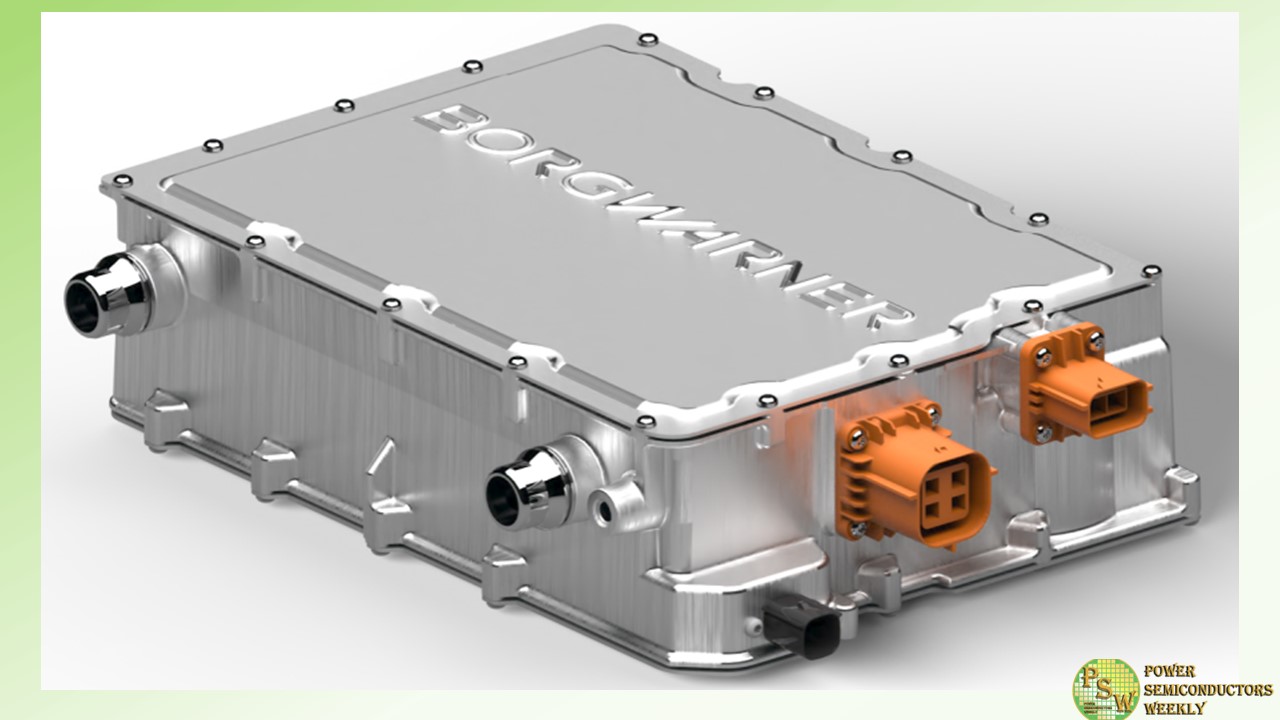
BorgWarner has clinched an agreement with a major North American OEM to supply its bi-directional 800V Onboard Charger (OBC) for the automaker’s premium passenger vehicle battery electric vehicle (BEV) platforms. The technology leverages silicon carbide (SiC) power switches for improved efficiency and delivers amplified power density, power conversion and safety compliance. Start of production is slated for January 2027.
“This is a big accomplishment for the team at BorgWarner, highlighting our first OBC win with this OEM and marks the first OBC win in North America,” said Dr. Stefan Demmerle, President and General Manager, BorgWarner PowerDrive Systems.
“Through our world-class power electronics expertise and market leading status for our 800-volt and silicon carbide technology, we are providing a solution to maximize charging power capabilities, extend power densities and enhance efficiencies while catering to differing grid configurations across regions.”
BorgWarner’s OBC technology is installed in electric vehicles to convert alternating current (AC) from the power grid to direct current (DC) to charge batteries. The OBC is capable of powers ranging from 19.2kW single-phase operation to 22kW three-phase operation.
The 19.2kW power level uses two power lines for a single-phase grid connection, which is unique to the U.S. market. The 22kW power level uses a three-phase grid connection and is intended for use in the European market. The 19.2kW single-phase charger is currently the only one of its kind to be introduced into the U.S. market.
The OBC incorporates a bi-directional vehicle-to-load (V2L) operating mode that enables users to use the vehicle battery pack to charge various standalone applications, which is an increasingly desired feature within the industry. Additionally, both the charger hardware and software are designed and produced by BorgWarner.
Original – BorgWarner
-
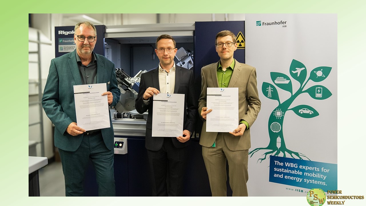
A cross-organizational team from Rigaku SE and Fraunhofer IISB has established a new semicon-ductor material characterization method in their jointly operated Center of Expertise for X-ray Topography in Erlangen, Germany. They succeeded not only in developing an industry-ready X-ray topography system, but also in employing defect detection and quantification algorithms, achieving a worldwide unique material characterization method for silicon carbide (SiC) wafers.
SiC is an excellent semiconductor for application areas like electric mobility and transportation, sustainable energy supply, industrial infrastructure up to sensors and quantum technologies even under harsh operating conditions.
As representatives for the whole research team, Dr. Kranert and Dr. Reimann from Fraunhofer IISB and Dr. Hippler, Managing Director Rigaku Europe SE, have won the Georg Waeber Innovation Award 2023 from the Förderkreis für die Mikroelektronik e.V. (Microelectronics Promotion Society).
Pioneering holistic material defect characterization with X-ray topography
In 2021, Rigaku SE and Fraunhofer IISB have founded the Center of Expertise for X-ray Topography, a joint lab that is located at the IISB’s headquarters in Erlangen, Germany. Here, the cross-organizational team has now developed a new metrology that is non-destructive, robust, reliable, high-throughput and therefore capable of swiftly detecting all relevant crystallographic defects in SiC substrates.
For the first time worldwirde, this innovation realized the holistic approach of setting up the measurement device, i.e., the X-ray topography (XRT) tool as well as formulating appropriate measurement and analysis routines that specifically meet the industry’s demands for speed, reliability, and accuracy. The development process was supported by rigorous scientific validation of the results, a crucial factor for the acceptance of a new approach in the industry.
Until now, no such industry-ready metrology existed for the early stages of SiC power electronics manufacturing, especially at substrate or crystal (commonly referred to as the “puck”) level. This breakthrough in SiC substrate inspection makes it no longer necessary to, e.g., destructively defect etch and discard semiconductor substrates for characterization, as is currently often the case. In consequence, the developed XRT metrology is superior to these existing substrate characterization methods employed in the industry, ultimately leading to substantial cost savings.
Effectively, this technology, developed in Germany, provides everything needed to become the industry standard for specifying and controlling substrate quality in production as well as for R&D substrate and device manufacturers worldwide. The success of this joint innovation is vividly illustrated by the new business, which Rigaku has successfully established in less than two years. Now, the Japan-based company is the world’s leading supplier of XRT tools for SiC substrate and device manufacturing.
The innovative metrology approach has been driven significantly by Dr. Michael Hippler, Managing Director of Rigaku Europe SE, and Dr. Christian Kranert with Dr. Christian Reimann, both group managers in the Fraunhofer IISB’s Materials department. Hence the scientists were selected for the Georg Waeber Innovation Award 2023 by the Förderkreis für die Mikroelektronik e.V. (Microelectronics Promotion Society).
The Förderkreis is an association of industry companies, two Fraunhofer institutes, four chairs of the University of Erlangen-Nuremberg and the Nuremberg Chamber of Commerce and Industry. The main objective is to foster a smooth exchange between science and industry, which is manifested in the Georg Waeber Innovation Award. The award is presented annually for outstanding scientific achievements and places a strong emphasis on the advancement of knowledge in microelectronics and its practical application in the industry. On October 25, 2023, Dr. Hippler, Dr. Reimann and Dr. Kranert received the award during a ceremony at Fraunhofer IISB in Erlangen.
Paving the way for the next generation of SiC power electronics
SiC semiconductor devices play a pivotal role in the power electronics industry. As a replacement for conventional silicon-based power electronics, SiC has the potential to enhance energy efficiency while reducing system costs. It is relevant across various application areas from electric mobility and transportation, sustainable energy supply, industrial infrastructure up to sensors and quantum technologies even under harsh operating conditions.
Consequently, processing low-cost, energy-efficient, and highly reliable SiC power devices is a critical endeavor with the worldwide electrification trend. The production capacities for SiC wafers experience significant growth, which goes hand in hand with an increasing demand for wafer inspection and metrology within the SiC industry. In particular, manufacturers of substrates and power devices require precice information regarding the quality of substrates in terms of crystallographic defects, their distribution across the entire wafer area, and absolute quantities.
Original – Fraunhofer IISB
-
“The 31st International Optoelectronics Exposition (OPTO Taiwan)”, organized by Photonics Industry & Technology Development Association, is taking place in Taipei Nangang Exhibition Hall 1 from October 25th to 27th, for a three-day technological extravaganza. As a leading company in semiconductor technology, GlobalWafers unveils its latest achievements in compound semiconductors.
At this year’s exposition, GlobalWafers features 8”N type SiC crystal growth technology, Thinning technology of 6”and 8”SiC wafers, and high-value niche products in the GaN epitaxy field, demonstrating its technical prowess honed over many years in the compound semiconductor industry. SiC crystal growth presents challenges due to the need for growth in extremely high-temperature sealed environments, with factors like hot zone design and crucible materials in crystal growth furnace adding the complexity to equipment and operations.
GlobalWafers independently designs and develops 8”SiC-specific Physical Vapor Transport Method Grower (PVT) to further reduce crystal growth costs while achieving higher material quality control. Through outstanding technical control and production efficiency, as well as continuous research and development, GlobalWafers overcomes the technical challenges of SiC crystal growth, successfully moving forward to 8 inches, providing customers with high-quality, superior-performance SiC materials.
The high hardness and brittleness of SiC make subsequent wafering process extremely challenging. Leveraging its edge in wafer processing, GlobalWafers has successfully developed SiC ultra-thin thinning technology, showcasing 6” 90µm and 8”350µm ultra-thin polished SiC wafers at the exhibition. Ultra-thin SiC wafers offer advantages in lightweighting, heat dissipation, thermal conductivity, high-frequency operation, component miniaturization, and material costs, making them an ideal choice for high-performance semiconductor devices.
GlobalWafers’ SiC wafers include 4”~ 6” semi-insulating wafers and 6”~ 8”conductive SiC wafers, offering a comprehensive range of products to cater for diverse customer needs and expand into various fields of application.
Heteroepitaxy of GaN poses various technical challenges, such as lattice mismatch, stress, and defects. GlobalWafers focuses on research and development, launching a full range of GaN heteroepitaxy products, including silicon, SiC and sapphire substrates. A variety of substrate selections can meet different requirements and expand terminal applications in an all-round way.
With its wealth of semiconductor substrate technology and years of industry experience, GlobalWafers has been able to give full play to our strengths and provide more advanced and high-efficiency solutions for the rapidly growing electric vehicle market.
Original – GlobalWafers
-
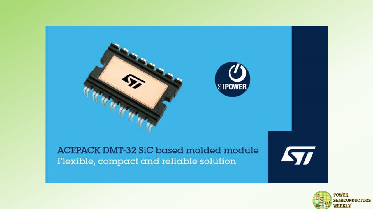
STMicroelectronics has released the ACEPACK DMT-32 family of silicon carbide (SiC) power modules in a convenient 32-pin, dual-inline, molded, through-hole package for automotive applications. Targeted at systems such as on-board chargers (OBC), DC/DC converters, fluid pumps and air conditioning, they deliver advantages including high power density, very compact design, and simplified assembly. The product family enhances flexibility for system designers by presenting a choice of four-pack, six-pack, and totem-pole configurations.
The modules contain 1200V SiC power switches that leverage ST’s state-of-the-art, second- and third-generation SiC MOSFET technology ensuring low RDS(on) values. The devices deliver efficient switching performance with minimal dependence on temperature to ensure high efficiency and reliability at converter system level.
Leveraging ST’s proven, robust ACEPACK technology, the modules reduce overall system- and design-development costs while ensuring outstanding reliability. The package technology features a high-performance aluminum nitride (AlN) insulated substrate for excellent thermal performance. There is also an integrated NTC sensor that provides temperature monitoring for thermal protection.
The first product in ACEPACK DMT-32, introduced today with ramp-up to volume production since Q4’23, is M1F45M12W2-1LA. The M1F80M12W2-1LA, M1TP80M12W2-2LA, M1P45M12W2-1LA, M1P80M12W2-1LA, M1P30M12W3-1LA are sampling now with ramp-up to volume production starting from Q1’24.
Original – STMicroelectronics
-
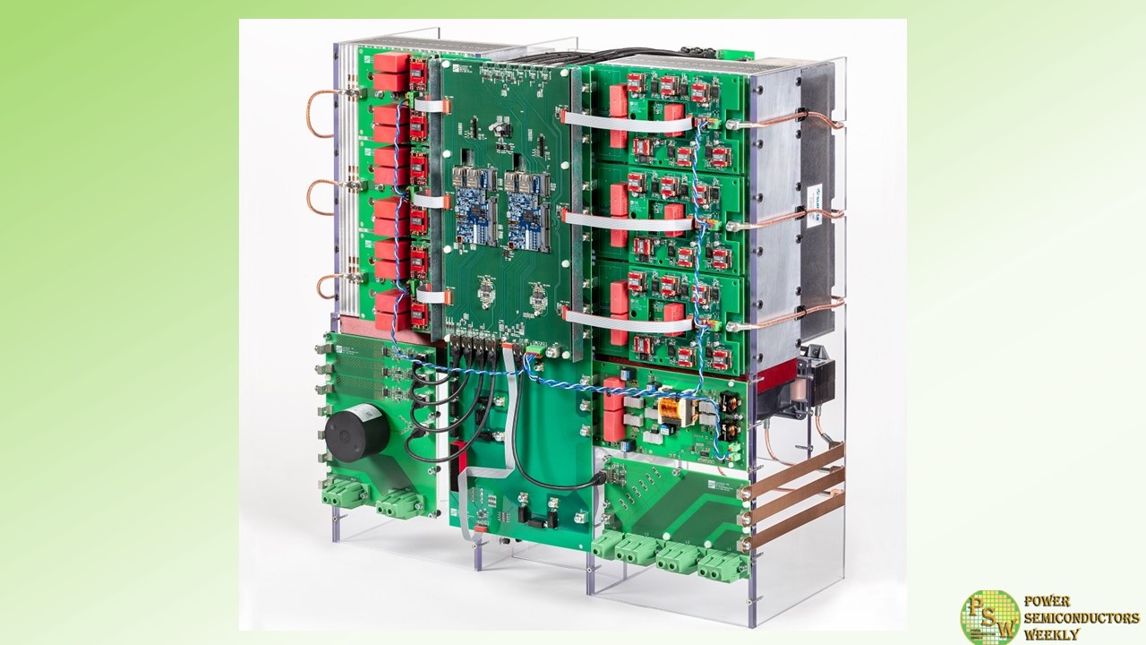
The Fraunhofer Institute for Solar Energy Systems ISE has developed and suc-cessfully commissioned the world’s first medium-voltage string inverter for large-scale power plants. By feeding power into the medium-voltage grid, the “MS-LeiKra” project team has demonstrated that PV inverters are technically capable of handling higher voltage levels.
The benefits for photovoltaics in-clude enormous cost and resource savings for passive components and cables. The device lays the foundation for a new system concept for the next genera-tion of large-scale PV power plants, which can also be applied to wind turbines, electric mobility and industrial applications.
Modern PV string inverters have an output voltage of between 400 VAC and 800 VAC. Although the output of power plants is steadily growing, voltage has not yet been increased. There are two reasons for this: First, building a highly efficient and compact inverter based on silicon semiconductors is a challenge. Second, there are currently no PV-specific standards that cover only the low-voltage range (max. 1,500 VDC / 1,000 VAC).
In a project funded by the German Federal Ministry for Economic Affairs and Climate Action (BMWK), Fraunhofer ISE, in collaboration with Siemens and Sumida, has developed an inverter that enables the output voltage to be increased to the medium-voltage range (1,500 V) at 250 kVA. The key to this is the use of silicon carbide semiconductors, which have a higher blocking voltage.
The research team has also implemented a more efficient cooling concept using heat pipes, which reduces the amount of aluminum required.
Thinner cables offer huge savings potential
An average photovoltaic power plant requires dozens of kilometers of copper cables. Increasing the voltage generates significant savings potential: At today’s possible output voltage of 800 VAC, a 250 kVA string inverter requires cables with a minimum cross section of 120 mm². By increasing the voltage to 1,500 VAC, the cable cross section can be reduced to 35 mm².
This in turn cuts copper consumption by around 700 kilograms per kilometer of cable. “Our resource analyses show that in the medium term, the electrification of the energy system will lead to copper becoming scarce. Increasing the voltage allows us to save valuable resources,” says Prof. Dr. Andreas Bett, Director of the Fraunhofer Institute for Solar Energy Systems ISE.
Standards need to change
With the “MS LeiKra” project, we are leaving the scope of low-voltage (<1000 VAC / <1500 VDC) standards. There are currently no PV-specific standards for this range. This is why the project team is also working on the standards that would result from increasing the voltage.
Finding a demo project partner
Having fed power into the medium-voltage grid successfully, the research team is now looking for solar farm developers and grid operators to test the power plant concept in the field.
Besides photovoltaics, moving beyond low voltage is also of interest for other applications, such as wind turbines, where the growing system capacities also require cables with large cross sections. The same is true for the charging infrastructure for large electric vehicles and vehicle fleets, and for industrial grids, where medium-voltage inverters could save a lot of material if cable cross sections could be reduced.
Original – Fraunhofer ISE
-

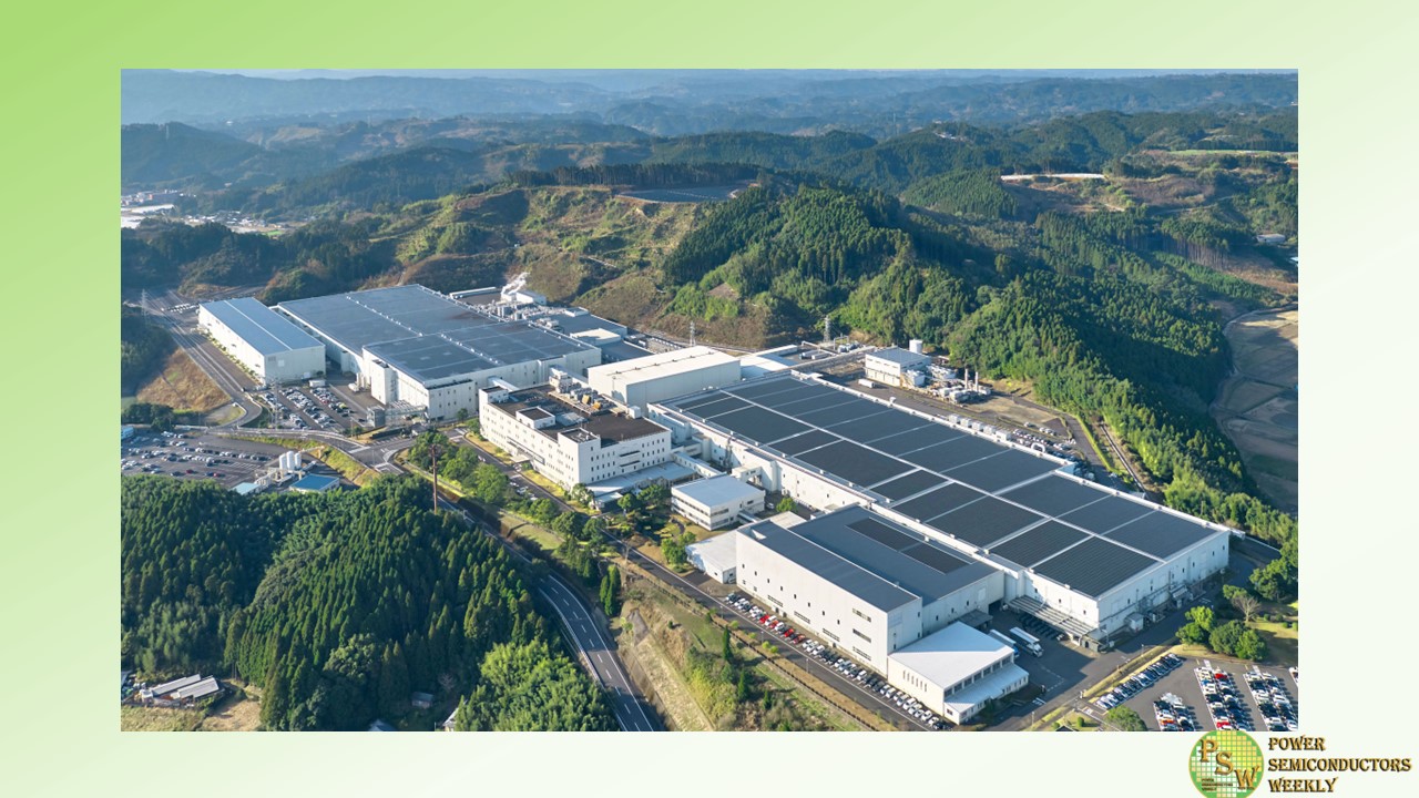
onsemi announced the completed expansion of its state-of-the-art, world-largest silicon carbide (SiC) fabrication facility in Bucheon, South Korea. At full capacity, this fab will be able to manufacture more than one million 200 mm SiC wafers per year.
To support the ramp in SiC manufacturing capacity, onsemi plans to hire up to 1,000 local employees over the next three years to fill the mostly highly technical positions – a more than 40% increase over the present workforce of about 2,300.
Silicon carbide devices are a critical component for power conversion in electric vehicles (EVs), energy infrastructure and high-power EV chargers. The rapidly growing demand for these products has created a surge in demand for SiC chips, with demand outpacing supply for the foreseeable future. The expansion of the Bucheon fab addresses the pressing need for additional production capacity, allowing onsemi to continue to provide supply assurance for its customers and strengthen its leadership in intelligent power solutions.
Construction of the new advanced 150 mm/200 mm SiC fab line along with the high-tech utility building and adjacent parking garage began in the middle of 2022 and was completed in September 2023. The expansion of the 150 mm/200 mm SiC Epi and wafer fab emphasizes onsemi’s focus on building out its vertically integrated silicon carbide manufacturing supply chain at brownfield locations. The Bucheon SiC line is starting with the production of 150 mm wafers and will be converted to 200 mm in 2025 upon qualification of the 200 mm SiC process.
onsemi’s leadership was joined by a delegation of dignitaries led by Vice Governor for Economy of the Gyeonggi-Do Taeyoung Yeom; followed by Bucheon City Mayor YongEek Cho; National Assembly delegates; and Bucheon Chamber of Commerce and Industry Chairman JongHuem Kim. Also in attendance were representatives from local communities, customers, suppliers and the semiconductor industry.
onsemi CEO Hassane El-Khoury opened the event, noting, “The 150 mm/200 mm SiC wafer fab in Bucheon is critical to the continued success of our fully integrated SiC supply chain, enabling us to support the acceleration of electrification globally. The last five years have shown what extraordinary performance our Bucheon team is capable of, and what we can achieve when we work together with governmental agencies toward the common goal of a more sustainable future.”
“I am truly impressed by onsemi’s diligent and yet fast execution of its strategic plan to expand the Bucheon SiC wafer fab,” said Bucheon City Mayor YongEek Cho. “Not only will the city of Bucheon benefit from the creation of new employment opportunities in technology, but it will also be a part of laying the foundation for a sustainable ecosystem through electrification.”
Original – onsemi
