-

Mitsubishi Electric Corporation will begin developing a prototype to demonstrate a junction-temperature estimation technology for power modules, which it is pursuing as a partner in the European Union’s Horizon Europe project aimed at developing advanced power modules and improving cost efficiency of renewable-energy power-generation.
The company is participating through its European subsidiary Mitsubishi Electric R&D Centre Europe B.V., which has joined the project, called Flagship Advanced Solutions for Condition and Health Monitoring in Power Electronics (FLAGCHIP).
In the global effort to expand the introduction of renewable energy to support carbon neutrality, the need to upgrade the reliability and maintenance of electronic devices for power conversion has become increasingly important. In particular, attention is being focused on technological innovations aimed at strengthening power module reliability and improving data acquisition and analysis methods to accurately determine degradation conditions in order to carry facilitate more timely maintenance.
The FLAGCHIP project currently involves 11 companies and academic institutions from nine European countries engaged in developing advanced power modules, condition and health monitoring technologies, and devising methods for calculating cost efficiency of renewable-energy power-generation systems and reducing associated costs. Demonstrations of wind-power and solar-power generation systems using these technologies and methods will be conducted at test facilities owned by project partners in Norway and France.
Mitsubishi Electric will be in charge of demonstrating a technology that estimates the junction temperature of silicon carbide metal-oxide-semiconductor field-effect transistor (SiC-MOSFET) semiconductor chips inside the power module, which will provide necessary data for accurately estimating module degradation.
Starting in October 2026, the demonstration will use the newly developed prototype at a test facility in France where direct current (DC) voltage is converted to a specific DC voltage for a wind-power generation system.
Original – Mitsubishi Electric
-

FORVIA HELLA, an international automotive supplier, has selected the new CoolSiC™ Automotive MOSFET 1200 V from Infineon Technologies AG for its next generation 800 V DCDC charging solution. Designed for on-board charger and DCDC applications in 800 V automotive architectures, Infineon’s CoolSiC MOSFET comes in a Q-DPAK package. The device uses top-side cooling (TSC) technology, which enables excellent thermal performance, easier assembly and lower system costs.
“We are excited to continue our partnership with FORVIA HELLA, leveraging our high-efficiency SiC products based on TSC packages,” said Robert Hermann, Vice President of Automotive High-Voltage Chips and Discretes at Infineon. “We are continuously working to take e-mobility to the next level by providing state-of-the-art SiC solutions that meet the automotive industry’s stringent requirements for performance, quality, and system cost.”
“Our customers are at the center of our efforts. That is why we have chosen Infineon’s CoolSiC Automotive MOSFET 1200 V for our next generation of DCDC converters”, said Guido Schütte, Member of the Electronics Executive Board at FORVIA HELLA. “Together with Infineon, we will continue to offer sustainable and innovative products and comprehensive services that exceed our customers’ expectations and drive the development of advanced mobility.”
Infineon’s new CoolSiC Automotive MOSFET 1200 V in the Q-DPAK package is based on Gen1p technology and offers a drive voltage in the range of V GS(off)= 0 V and V GS(on)= 20 V. The 0 V turn-off enables unipolar gate control, which simplifies design by reducing the number of components in the PCB.
With a creepage distance of 4.8 mm, the package achieves an operating voltage of over 900 V without the need for additional insulation coating. Compared to backside cooling, the TSC technology ensures optimized PCB assembly, reducing parasitic effects and resulting in significantly lower leakage inductances. As a result, customers benefit from lower package parasitics and lower switching losses. Heat dissipation is further improved by diffusion soldering the chip with .XT technology.
Original – Infineon Technologies
-

Vishay Intertechnology, Inc. introduced 16 new 650 V and 1200 V silicon carbide (SiC) Schottky diodes in the industry-standard SOT-227 package. Designed to deliver high speed and efficiency for high frequency applications, the Vishay Semiconductors devices offer the best trade-off between capacitive charge (QC) and forward voltage drop for diodes in their class.
The devices consist of 40 A to 240 A dual diode components in a parallel configuration, and 50 A and 90 A single phase bridge devices. Built on state of the art thin wafer technology, the diodes feature a low forward voltage drop down to 1.36 V that dramatically reduces conduction losses for increased efficiency. Further increasing efficiency, the devices offer better reverse recovery parameters than Si-based diodes and have virtually no recovery tail.
Typical applications for the components will include AC/DC PFC and DC/DC ultra high frequency output rectification in FBPS and LLC converters for photovoltaic systems, charging stations, industrial UPS, and telecom power supplies. In these applications, the diodes’ low QC down to 56 nC allows for high speed switching, while their industry-standard package offers a drop-in replacement for competing solutions.
The diodes deliver high temperature operation to +175 °C and a positive temperature coefficient for easy parallelling. UL-approved to file E78996, the devices feature a large creepage distance between terminals and a simplified mechanical design for rapid assembly.
Original – Vishay Intertechnology
-

Wolfspeed, Inc. introduced its new Gen 4 technology platform, which enables design rooted in durability and efficiency, all while reducing system cost and development time. Engineered to simplify switching behaviors and design challenges commonly experienced in high-power designs, Gen 4 charts a long-term roadmap across Wolfspeed’s product categories, including power modules, discrete components, and bare die products. These products are currently available in the 750V, 1200V and 2300V classes.
“We understand that each application’s design comes with a unique set of requirements,” said Jay Cameron, senior vice president of Wolfspeed power products. “From its inception, our goal for Gen 4 has been to improve overall system efficiency in real-world operating environments, with a focus on delivering maximum performance at the system level. Gen 4 enables design engineers to create more efficient, longer-lasting systems that perform well in tough operating environments at a better overall system cost.”
Silicon carbide technology is one of the fastest growing components of both the power device market and the greater semiconductor industry. A superior alternative to silicon, silicon carbide is ideal for high power applications – such as EV powertrains, e-mobility, renewable energy systems, battery energy storage systems, and AI data centers – that unlocks improved performance and lower system costs.
As the U.S. and the globe pursue more efficient and environmentally friendly solutions to meet the world’s ever-increasing need for high-voltage energy sources, it is crucial that the U.S. continue to make strategic investments to cement its technological dominance, while continuing to spur American innovation in critical technologies.
Wolfspeed is the only silicon carbide producer with both silicon carbide material and silicon carbide device fabrication facilities based in the United States, a factor that is becoming increasingly important under the new U.S. Administration’s increased focus on national security and investment in U.S. semiconductor production.
“Innovative technology unlocks business opportunity,” said Devin Dilley, president and chief product officer, EPC Power, a U.S.-based utility-scale inverter manufacturer. “Wolfspeed’s new Gen 4 SiC technology is enabling EPC Power to make a paradigm shift in how energy is created and stored globally.”
“As the world-leader in silicon carbide technology, based on American IP and delivered through U.S.-based fabrication facilities, Wolfspeed has been relentless in our drive to continue to innovate and bring our silicon carbide solutions to more and more industries with increasingly challenging use cases,” said Wolfspeed Executive Chairman, Tom Werner. “Our Gen 4 platform will be delivered via our highly efficient 200mm wafers, which will enable us to deliver products on a scale and level of yield not seen in this industry before.”
Wolfspeed’s Gen 4 platform was designed to comprehensively improve system efficiency and prolong application life, even in harshest of environments, while helping to reduce system cost and development time. The technology will deliver significant performance enhancements for designers of high-power automotive, industrial, and renewable energy systems, with key benefits including:
- Holistic System Efficiency: Delivering up to a 21% reduction in on-resistance at operating temperatures with up to 15% lower switching losses.
- Durability: Ensuring reliable performance, including a short-circuit withstand time of up to 2.3 µS to provide additional safety margin.
- Lower System Cost: Streamlining design processes to reduce system costs and development time.
Learn more in Wolfspeed’s white paper “Gen 4 Silicon Carbide Technology: Redefining Performance and Durability in High-Power Applications”.
Wolfspeed’s Gen 4 products are available in 750V, 1200V and 2300V nodes, with options for power modules, discrete components, and bare die products. New product introductions, including additional footprints and RDSON ranges, will be available throughout 2025 and early 2026.
Original – Wolfspeed
-
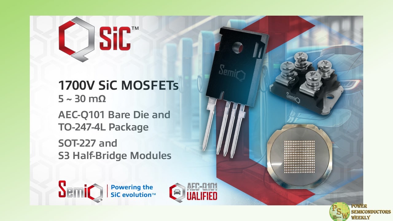
SemiQ Inc. announced a family of 1700 V SiC MOSFETs designed to meet the needs of medium-voltage high power conversion applications, such as photovoltaic and wind inverters, energy storage, EV and road-side charging, uninterruptable power supplies, and induction heating/welding.
The high-speed QSiC™ 1700 V switching planar D-MOSFETs enable more compact system designs at large scale, with higher power densities and lower system costs. They feature a reliable body diode, capable of operation at up to 175oC, with all components tested to beyond 1900 V, and UIL avalanche tested to 600 mJ.
The QSiC 1700 V devices are available in both a bare die form (GP2T030A170X), and as a 4-pin TO-247-4L-packaged discrete (GP2T030A170H) with drain, source, driver source and gate pins. Both are also available in an AEC-Q101 automotive qualified version (AS2T030A170X and AS2T030A170H).
The MOSFETs deliver low switching and conduction losses, low capacitance and feature a rugged gate oxide for long-term reliability, with 100 percent of components undergoing wafer-level burn in (WLBI) to screen out potentially weak oxide devices.
SemiQ has also announced a series of three modules as part of the family to simplify system design, this includes a standard-footprint 62 mm half-bridge module housed in an S3 package with an AIN insolated baseplate, as well as two SOT-227 packaged power modules.
The QSiC 1700 V series’ bare die MOSFET comes with an aluminum (Al) top side and nickel/silver (Ni/Ag) bottom side. Both it and the TO-247-4L packaged device have a power dissipation of 564 W, with a continuous drain current of 83 A (at 25oC, 61A at 100oC) and a pulsed drain current of 250 A (at 25oC). They also feature a gate threshold voltage of 2.7 V (at 25oC, 2.1 V at 125oC), an RDSON of 31 mΩ (at 25oC, 57 mΩ at 125oC), a low (10n A) gate source leakage current and a fast reverse recovery time (tRR) of 17 ns. The TO-247-4L package has a junction to case thermal resistance of 0.27oC per watt.
The two 4-pin power modules are housed in a 38.0 x 24.8 x 11.7 mm SOT-227 design and deliver an increased power dissipation of 652 W with an increased continuous drain current of 123 A (at 25oC – GCMX015A170S1E1) and 88 A (at 25oC GCMX030A170S1-E1). In addition to low switching losses, both modules have a low junction-to-case thermal resistance of 0.19oC and 0.36oC per watt and feature an easy-mount design for direct mounting of the isolated package to a heatsink.
The half-bridge module is housed in a 61.4 x 106.4 x 30.9 mm 9-pin S3 package and delivers a power dissipation of 2113 W with a continuous drain current of 397 A and a pulsed drain current of 700 A. In addition to low switching losses, the GCMX005A170S3B1-N module has a junction to case thermal resistance of 0.06oC per watt.
Original – SemiQ
-

onsemi announced that it has completed its acquisition of the Silicon Carbide Junction Field-Effect Transistor (SiC JFET) technology business, including the United Silicon Carbide subsidiary, from Qorvo for $115 million in cash.
The addition of SiC JFET technology will complement onsemi’s extensive EliteSiC power portfolio and enable the company to address the need for high energy efficiency and power density in the AC-DC stage in power supply units for AI data centers.
In electric vehicle applications, SiC JFETs help improve efficiency and safety by replacing multiple components with a solid-state switch based on SiC JFET in battery disconnect units. In the industrial end-market, SiC JFETs enable certain energy storage topologies and solid-state circuit breakers.
“This acquisition further strengthens onsemi’s leadership in power semiconductors by providing disruptive and market leading technologies to our customers to solve their most pressing power density and efficiency problems in AI data centers, automotive and industrial markets,” said Simon Keeton, group president and general manager of the Power Solutions Group, onsemi. “We will continue to innovate and make investments to expand our technology leadership in providing the most comprehensive power system solutions.”
Original – onsemi
-

X-FAB Silicon Foundries SE has launched XSICM03, its next-generation XbloX platform, advancing Silicon Carbide (SiC) process technology for power MOSFETs, delivering significantly reduced cell pitch, enabling increased die per wafer and improved on-state resistance without compromising reliability.
XbloX is X-FAB’s streamlined business process and technology platform designed to accelerate the development of advanced SiC MOSFET technology. It integrates qualified SiC process development blocks and modules for planar MOSFET production, simplifying the onboarding process and significantly reducing design risks and product development time.
By combining proven process modules with robust design rules, control plans, and FMEAs, XbloX enables faster prototyping, easier design evaluation, and shorter time to market. This approach gives customers a competitive edge, allowing designers to create a diverse product portfolio while achieving production timelines up to nine months faster than traditional development methods.
This next generation platform provides active area design cell size reduction while maintaining robust process controls, as well as leakage and breakdown device performance. The XSICM03 platform with robust design rules allows customers to create SiC planar MOSFETs with a cell pitch that is over 25% smaller than the previous generation.
This improvement allows for up to a 30% increase in die per wafer compared to the previous generation. Leveraging proven process blocks, the platform ensures exceptional gate oxide reliability and device robustness. The enriched PCM library and enhanced design support allow for fast customer tape-out, resulting in faster product development.
Rico Tillner, CEO, X-FAB Texas explains: “With its streamlined approach, our next-generation process platform addresses the increasing demand for high-performance SiC devices in automotive, industrial, and energy applications. We enable existing and new customers in creating application-optimized product portfolios through accelerated prototyping and design evaluation, significantly reducing time to market.”
The next generation platform XSICM03 is now available for early access.
Original – X-FAB Silicon Foundries
-

Bosch has signed a preliminary memorandum of terms (PMT) under the CHIPS and Science Act with the U.S. Department of Commerce (DoC). It includes up to $225 million in proposed direct funding to support the transformation of the Bosch production facility in Roseville, California. The proposed investment would support the development of semiconductor manufacturing in the U.S. Bosch plans to invest up to $1.9 billion to transform the Roseville site into a facility that produces and tests silicon carbide (SiC) semiconductors. The Roseville site currently employs around 250 associates with potential to grow in the future.
In April 2023, Bosch announced its intention to acquire the assets of an existing wafer fab in Roseville. The acquisition was closed in August 2023 and since that time Bosch has begun the process to transform the site. Starting in 2026, the first chips will be produced on 200-millimeter wafers based on the pioneering SiC Bosch technology.
“Production of SiC chips in the United States is a key part of our strategic plan to reinforce our semiconductor portfolio and support our local customers,” said Michael Budde, president of Mobility Electronics for Bosch. “Silicon carbide chips help to enable greater range and more efficient recharging in battery-electric vehicles and plug-in hybrid vehicles to provide affordable electromobility options for consumers.”
The Roseville location has nearly 40 years of extensive experience in the design and production of semiconductors for automotive and industrial applications.
“We took the unique approach to transform an existing wafer fab rather than build a new facility,” said Thorsten Scheer, plant manager in Roseville and regional president of the Bosch Mobility Electronics division in North America. “A major reason was the talented workforce in place at Roseville. Already they have shown their skill and resolve as we transform the site for future production of silicon carbide chips.”
Since the acquisition of the site, Bosch has retained nearly all of the 250 associates during the transformation process as it prepares for the 2026 launch of SiC production. The company has provided advanced training where the Roseville team learns from other sites within the Bosch global manufacturing network.
In addition to training its current workforce, Bosch is also investing locally to help build up semiconductor expertise for the future. The Bosch Community Fund provided a $100,000 grant to the Sierra College Foundation in Rocklin, California for its Career Technical Education Support Fund. The grant has helped to support associated costs with certification fees, microcontroller kits, development material, software, protective gear, tools, entry and travel fees for STEM competitions, project supplies for STEM Clubs and more.
The Roseville site represents the first semiconductor production site in the United States for Bosch. Over the next years, the company intends to invest around $1.9 billion USD in the Roseville site and upgrade the manufacturing facilities to state-of-the-art processes. Proposed investment from the CHIPS and Science Act would help support the transformation of the site. Already the site has received a $25 million California Competes Tax Credit incentive from the Governor’s Office of Business & Economic Development (GO-Biz) to support redevelopment and investment in Roseville.
Bosch has indicated it plans to claim the Department of the Treasury’s Advanced Manufacturing Investment Credit (CHIPS ITC), which is 25% of qualified capital expenditures. Click here to learn more about the tax credit. In addition to the proposed direct funding of up to $225 million, the CHIPS Program Office would make approximately $350 million in proposed loans – which is a part of the $75 billion in loan authority provided by the CHIPS and Science Act – available to Bosch under the PMT.
As explained in its first Notice of Funding Opportunity, the Department of Commerce may offer applicants a PMT on a non-binding basis after satisfactory completion of the merit review of a full application. The PMT outlines key terms for a potential CHIPS incentives award, including the amount and form of the award. The award amounts are subject to due diligence and negotiation of award documents and are conditional on the achievement of certain milestones. After a PMT is signed, the Department of Commerce begins a comprehensive due diligence process on the proposed projects and continues negotiating or refining certain terms with the applicant. The terms contained in any final award documents may differ from the terms of the PMT being announced.
Original – Bosch
-

onsemi has unveiled plans to acquire Qorvo’s Silicon Carbide (SiC) JFET business, a strategic move that enhances its portfolio in high- and mid-voltage power semiconductors. The $115 million deal includes Qorvo’s United Silicon Carbide subsidiary and is expected to close in Q1 2025. This acquisition is projected to expand onsemi’s market opportunity by $1.3 billion by 2030, focusing on AI, data centers, EVs, and industrial markets. By leveraging its vertically integrated SiC supply chain, onsemi aims to boost efficiency, profitability, and innovation across key technology areas.
SiC JFET technology offers superior power efficiency, reduced costs, and versatility in advanced applications, including EV battery systems, AI-driven data centers, and renewable energy solutions. It promises to disrupt traditional silicon-based and GaN technologies, with its superior switching speed, lower on-resistance, and smaller die size. This acquisition positions onsemi to capitalize on the growing demand for sustainable, high-performance power solutions in a wide range of industries.
Moreover, SiC JFETs are designed to enable transformative advancements in industrial applications such as power supplies, solar power converters, and energy storage systems. These innovations align with market trends emphasizing higher efficiency and reliability. The technology also offers critical advantages in EV battery safety, ensuring quicker response and long-term dependability through solid-state switches that surpass conventional electromechanical solutions.
By integrating Qorvo’s business, onsemi also strengthens its presence in the competitive AI and data center markets. The shift to higher voltages and power capacities in these areas provides a unique opportunity for SiC JFETs to reduce costs and improve performance, establishing onsemi as a leader in next-generation semiconductor solutions.
Original – onsemi
-

ROHM has announced the adoption of its EcoSiC™ products, including SiC MOSFETs and SiC Schottky barrier diodes (SBDs) in the HFA/HCA series of 3.5kW output AC-DC power supply units for 3-phase applications from COSEL, a leading power supply manufacturer in Japan. Incorporating ROHM SiC MOSFETs and SiC SBDs into the forced air-cooled HFA series and conduction-cooled HCA series achieves up to 94% efficiency. The HCA series has been mass produced since 2023, while the HFA series began mass production in 2024.
Many industrial applications that handle high power in the industrial sector, including MRI machines and CO2 lasers, require 3-phase power supplies that differ from the single-phase power supplies used in households. COSEL’s AC-DC power supply units – equipped with ROHM’s EcoSiC™ technology that excels in high-temperature, high-frequency, high-voltage environments – are compatible with 3-phase power supplies from 200VAC to 480VAC, contributing to improved power supply efficiency across a wide range of industrial equipment worldwide.
Jun Uchida, General Manager, New Product Development Dept. 2, COSEL Co., Ltd.
“The HFA/HCA series achieve high efficiency despite delivering a high-power output of 3.5kW by incorporating ROHM’s low-loss SiC power devices. Operating at high input voltages typically poses a challenge in reducing losses in high-voltage power devices, but using SiC power devices translates to significantly lower losses compared to conventional solutions, resulting in power supplies that maintains high efficiency and power density even under demanding high-power conditions.”
Akihiro Hikasa, Group General Manager, Power Devices Business Unit, SiC Business Section, ROHM Co., Ltd.
“We are delighted to support COSEL, an industry leader in power supply systems, by providing SiC power devices. A leading company in SiC power devices, ROHM also provides comprehensive power solutions that combine peripheral components. In addition, by addressing customer issues, we also improve device performance by incorporating the insights gained into our products. Going forward, we will continue to collaborate with COSEL to contribute to a sustainable society by enhancing the efficiency of industrial equipment that handle large amounts of power.”
The HFA/HCA series are 3.5kW power supplies featuring a wide input range (200VAC to 480VAC) that meets global power supply requirements. This allows them to be used anywhere in the world without the need to modify the power supply for each region, contributing to the standardization of application designs. Both forced air-cooled (HFA series) and conduction-cooled (HCA series) models – selectable based on operating environment – are available in 48V and 65V output voltage variants that can be used as power sources for a variety of high-power applications such as laser generation and MRI.
Original – ROHM
