-

Revasum, Inc. announced a strategic partnership with SGSS, a global leader in high-performance materials and innovative solutions. This partnership aims to revolutionize the semiconductor industry by developing a cutting-edge line of grinding wheels specifically designed for Silicon Carbide (SiC) wafers.
Silicon Carbide is a critical material in the production of power devices and has gained significant prominence in the semiconductor industry due to its exceptional properties. The demand for SiC wafers has been steadily growing, and achieving the highest quality wafers is paramount to meet the evolving needs of the market.
The partnership between Revasum and SGSS represents a collaboration between two industry giants with a shared commitment to innovation and excellence. By combining Revasum’s expertise in semiconductor manufacturing equipment with SGSS’s cutting-edge abrasive materials, this alliance seeks to develop a new generation of surface finishing solutions that will set new standards for precision, efficiency, and surface quality in SiC wafer production with sustainability and environmental responsibility at the core of our collaboration.
This partnership holds great promise for the semiconductor industry, paving the way for enhanced SiC wafer production processes that will contribute to the advancement of power electronics, electric vehicles, renewable energy, and various other technology sectors.
Mr. Scott Jewler, CEO of Revasum, Inc., commented on the partnership, saying, “We are excited to join forces with Saint-Gobain Surface Solutions, a renowned leader in materials science and innovation. This partnership will enable us to provide our customers with cutting-edge tools and solutions to address the increasing demand for high-quality Silicon Carbide wafers.”
Mr. Jean-Claude Lasserre, CEO Saint-Gobain Surface Solutions stated, “Our collaboration with Revasum exemplifies our commitment to delivering high-performance materials and solutions that push the boundaries of what is possible. Together, we will unlock new levels of precision and efficiency in Silicon Carbide wafer grinding with highest levels of sustainable products and solutions.”
Both Revasum, Inc. and SGSS are eager to embark on this journey of innovation and look forward to delivering groundbreaking solutions that will shape the future of Silicon Carbide wafer manufacturing.
Original – Revasum
-
Solitron Devices has acquired Micro Engineering Inc. located in Apopka, FL. Specializing in highly integrated, high reliability assemblies, Micro Engineering has over forty years of experience servicing medical, industrial, and aerospace applications.
Focused on low to mid volume production, Micro Engineering offers services from conceptual design and prototyping to full turnkey manufacturing and functionally tested assemblies. Additional services include hand assembly, wire harnessing, specialized coatings and full box builds.
Mark Matson, Solitron President & COO, said, “Micro Engineering is an exceptionally synergistic fit with Solitron, expanding and complimenting engineering and manufacturing capabilities. Solitron’s expertise with chip and wire, silicon carbide and high-density multi-chip modules combined with Micro Engineering’s PCBA, SMT and system level box build capability offers a strong suite of technology to customers.
This new capability for increased functionality and power density will accelerate introductions into emerging markets particularly utilizing Silicon Carbide (SiC) and Gallium Nitride (GaN). The combination of Solitron and Micro Engineering will also broaden both companies’ presence in medical, high end industrial and aerospace applications.”
Combined manufacturing capabilities now include 3D CAD modelling, 3D Printing, CAE machining, aluminum & gold wire bonding, void free soldering, fine pitch SMT for BGA’s, rigid, flex and double-sided circuit card assemblies; right up through full box builds. Product qualification infrastructure includes thermal shock, vibration, mechanical shock, centrifuge, salt spray atmosphere, burn-in and more. Micro engineering is ISO-9001 registered.
Original – Solitron Devices
-
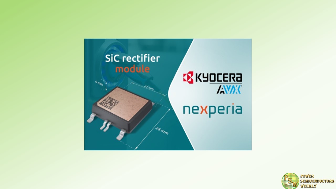
Nexperia has entered into partnership with KYOCERA AVX Components (Salzburg) GmbH to jointly produce a new 650 V, 20 A silicon carbide (SiC) rectifier module for high frequency power applications ranging from 3 kW to 11 kW power stack designs, aimed at application like industrial power supplies, EV charging stations, and on-board chargers. This release will represent a further deepening of the existing, long-lasting partnership between the two companies.
Space-saving and weight reduction are the key requirements for manufacturers of the next generation power applications. The compact footprint of this new SiC rectifier module will help to maximize power density, thereby reducing the amount of required board space and lowering the overall system cost.
Thermal performance is optimized using a combination of top-side cooling (TSC) and an integrated negative temperature coefficient (NTC) sensor which monitors the device temperature and provides real time feedback for device or system level prognosis and diagnosis. This rectifier module has a low inductance package to enable high frequency operation and it has been qualified to operate with a junction temperature of up to 175 °C.
“This collaboration between Nexperia and KYOCERA AVX combines cutting edge silicon carbide semiconductors with state-of-the-art module packaging and will allow Nexperia to better serve the market demand for power electronic products which offer exceptionally high levels of power density,” according to Katrin Feurle, Senior Director of the Product Group SiC at Nexperia. “The release of this rectifier module will represent the first step in what is envisaged as a long-term SiC partnership between Nexperia and KYOCERA AVX”.
Thomas Rinschede, Deputy Vice President Sensing and Control Division at KYOCERA AVX Components Sensing and Control Division, comments: “We are delighted to further extend our successful partnership with Nexperia into the production of silicon carbide modules for power electronics applications. Nexperia’s manufacturing expertise combined with KYOCERA module know-how make a compelling offering for customers looking to achieve higher power densities using wide bandgap semiconductor technology.”
Nexperia expects samples of the new SiC rectifier modules to be available in the first quarter of 2024.
Original – Nexperia
-

Yield Engineering Systems, Inc. (YES), a leading manufacturer of process equipment for semiconductor, life sciences, and “More-than-Moore” applications, had sold multiple Wet Processing Systems to a premier Silicon Carbide (SiC) materials manufacturer. The adoption of SiC Wide Band Gap (WBG) semiconductors continues to grow with demand driven by Electric Vehicle (EV) production and charging infrastructure, power supply systems, and Photovoltaic (PV) inverters.
The YES TersOnus™ wet solution continues to gain momentum in the SiC market. YES’ highly flexible and custom-configured systems have superior temperature uniformity complimented by ultra-low particle performance. These systems can address 150mm and 200mm Silicon Carbide processes without process downtime or line changes.
“Silicon carbide materials manufacturers are seeking technology partners that provide specific solutions to their roadmap challenges. TersOnus™ for post epitaxial & chemical mechanical polishing (CMP) wet cleaning addresses these specific needs by providing unparalleled process efficacy, automated handling capabilities, and adaptable system configurations with significant Cost of Ownership advantages. This multi-tool order validates YES’ efforts to serve our SiC customers and allow them to go to market quickly with proven HVM solutions.” said Dragan Cekic, VP of Strategic Sales for YES,
“YES has a rich history of providing highly automated, customer-configured wet processing technology. YES is excited about our involvement in the rapidly growing global market for SiC devices. This order confirms our solutions’ value proposition for the broader SiC ecosystem,” said Kevin Trompak, Vice President of Business Development for YES. “YES is committed to supporting the development of SiC solutions by investing in an Advanced Technology Center in Chandler, Arizona, which officially opened July 27th this year.”
Original – Yield Engineering Systems
-
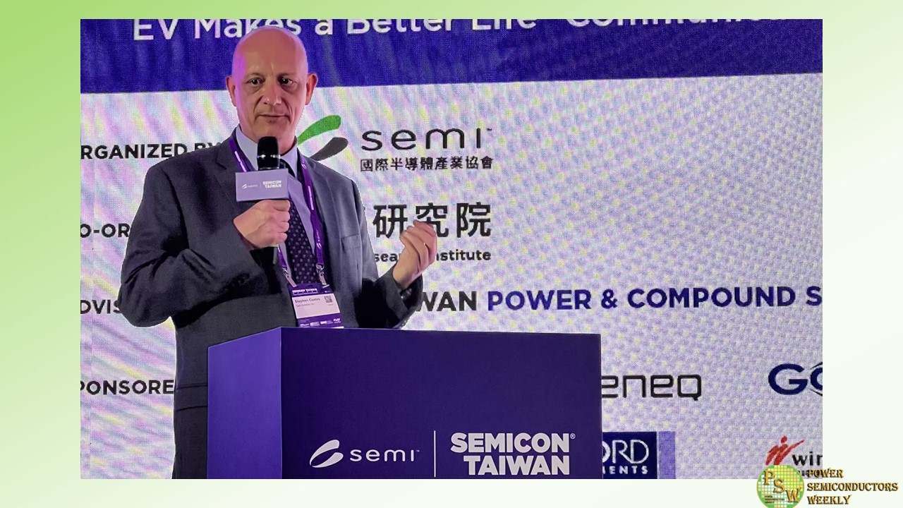
SEMICON Taiwan 2023 once again underscored Taiwan’s strategic importance in the global semiconductor industry. Entering its 28th year, the event was held in Taipei, gathering 950 exhibitors with 3,000 booths and attracting more than 62,000 visitors. The sheer scale of participation was evident in the hour-long traffic queues and bustling metro platforms as people flocked into the Exhibition Halls.
Innovations and sustainability were the focal points of this year’s show. Distinguished figures from the industry took the stage to emphasize the resilience of the semiconductor supply chain and envision a greener and more intelligent future enabled by semiconductors. Fueled by tremendous opportunities in artificial intelligence, communications, and automotive electronics, the semiconductor industry is poised to expand to a trillion-dollar market by the close of this decade despite the short-term cyclical downturns.
Reshaping Mobility with Power Semiconductors
This year, energy efficiency came to the forefront of innovations, especially among applications that have far-reaching impacts on the global economy, with electric vehicles being one.
Electrification and autonomous trends continue to drive up the semiconductor content per vehicle. Wide bandgap semiconductors like SiC and GaN have emerged as pivotal players, making substantial contributions to the performance and efficiency of next-generation electric vehicles.
It was exciting to see industry key players illustrate significant improvements achieved by new-generation semiconductors in terms of power efficiency, power density, and connectivity. Research firms estimate that silicon-based semiconductors will grow at a CAGR of 4% from 2022 to 2028, while SiC will grow at 31% and GaN at 49%, highlighting the growth potential of wide bandgap semiconductors.
More Data, More Computing Power, More Energy Consumption
The rapid adoption of artificial intelligence applications in every aspect of our lives presents a significant opportunity for the semiconductor industry. The recent breakthroughs in artificial intelligence, like generative AI, are made possible by the progress of semiconductor technologies, which were on full display at this year’s expo.
The computing power and the memory access required for AI applications are still growing at an unprecedented pace, and the energy consumption is proportional to the computing capability. More efficient energy conversion and distribution solutions are critical for data centers to accommodate increasing energy-intensive workloads.
Key takeaways Summary
- SEMICON Taiwan once again turned out to be an enlightening event, fostering the exchange of experiences and the dissemination of ingenious ideas.
- Energy efficiency challenges overall system performance as electronic devices become versatile and highly integrated. GaN power semiconductors are a low-cost and reliable solution to tackle power challenges for power-hungry applications.
- Technology advancement hinges on two significant investments: innovation and talent. We’re pleased to note these were repeatedly addressed in keynotes and presentations at this year’s event.
Original – GaN Systems
-
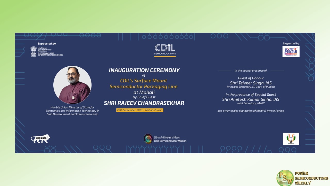
Hon’ble Union Minister of State for Electronics and Information Technology, Shri Rajeev Chandrasekhar, virtually inaugurated the new Surface Mount Semiconductor Packaging Line, at Continental Device India Private Limited’s (CDIL) Mohali plant today. With the new versatile SMA and SMB package line, via the Government of India’s SPECS, CDIL becomes India’s first Silicon Carbide components manufacturer, scaled to make auto-grade devices, including Silicon Carbide MOSFETs, Silicon Carbide Schottky Diodes, Rectifiers, Zeners and TVS Diodes among others for the global as well as the domestic market. The expansion of assembly lines will increase CDIL’s total capacity at the facility to 600 million units annually.
The new line inauguration was also attended by Shri Tejveer Singh, IAS, Principal Secretary, IT, Government of Punjab, and Shri Amitesh Kumar Sinha, IRAS, Joint Secretary, MeitY and other senior dignitaries of MeitY and Invest Punjab.
With the impending surge in electric vehicles (EVs), power management devices and solar-powered panels, globally as well as in India, and their increased reliance on wide band gap electronics, CDIL identified and laid focus on Silicon Carbide (SiC) products.
SiC is an emerging technology that allows for much-improved efficiencies and power-handling capabilities, especially in high-power charging applications and battery management systems. CDIL spent R&D efforts pursuing SiC technology so as to build proficiency and assist in the world’s switch to Electric Vehicles.
Expressing his gratitude, Tejveer Singh, IAS, Principal Secretary, IT, Government of Punjab, said, “I am very very thankful to the CDIL team for this great effort in expanding the plant capacity and assembly line. And as CDIL and SCL sign the MoU, we can finally see Mohali becoming the chip-making hub of India. The Government has a vision to cultivate a dynamic semiconductor ecosystem in Mohali and therefore, the modernization of SCL could provide the sector the much needed impetus to put Mohali on the semiconductor manufacturing map of India.”
Speaking at the launch of the new assembly lines, Amitesh Kumar Sinha, IRAS, Joint Secretary, MeitY, said, “India’s Semiconductor mission is a key focus for both the Union and the State Governments, and there have been many developments in the sector. Yet, India still has much to catch up, with a projected surge in demand to approximately $110 billion by 2030. At MeitY, our objective is to modernise and commercialise SCL with focus on making it a R&D hub for developing the semiconductor ecosystem in the country.
It’s heartening to see CDIL taking the lead in Packaging of discrete semiconductor devices. CDIL has capability for R&D, Design, and Packaging. Earlier, they also had a fabrication facility. I hope CDIL will also consider setting up a discrete fab in the country by availing financial support under the Semicon India programme in future. As CDIL and SCL join hands for knowledge exchange, India can look forward to more indigenous chip manufacturing and packaging for India and the world in the upcoming future.”
CDIL has also established an advanced testing and reliability laboratory at the Mohali plant. The facility, a one-of-a-kind in India, is equipped to meticulously qualify the semiconductor products according to the stringent standards stipulated by the Automotive Electronics Council (AEC), ensuring they meet the rigorous demands of the automotive domain.
Commenting on the same, Prithvideep Singh, General Manager, CDIL said, “In line with our steadfast commitment to innovation and market diversification, CDIL Semiconductors has strategically positioned itself to meet the burgeoning demands of the automotive sector, both within India and on a global scale. Even though SiC devices are notoriously hard to manufacture at scale, we have spent effort and investment to master them. CDIL has been able to innovate on the brittleness and complexity around the production of SiC devices and has earned the resounding approval of large multinational customers in export markets.”
CDIL also signed an MoU with the Semi-Conductor Laboratory (SCL), a research institute in Mohali under MeitY, undertaking research and development in the field of semiconductor technology. Both parties will aim to establish a comprehensive framework wherein SCL’s specialized knowledge and wafer fabrication facilities are utilized to produce indigenized wafers for CDIL’s discrete semiconductor devices, using CDIL’s proprietary manufacturing processes. This collaborative effort is aimed as a significant stride towards advancing India’s semiconductor ambitions in fostering a stronger, self-reliant industry in the region.
Silicon Carbide (SiC) material boasts a significantly wider bandgap compared to traditional semiconductor materials like silicon. A wide bandgap (~3.26 eV for SiC) enables SiC devices to operate at higher temperatures and handle higher breakdown voltages. Consequently, SiC emerges as the optimal choice for the electric vehicle (EV), power management and solar sectors, as it allows semiconductor components to operate reliably in high temperatures, reducing the need for complex cooling systems.
The company has already initiated pilot production in August with 50 million units and promptly delivered its inaugural batch to customers in both the domestic and international markets. CDIL operates manufacturing facilities and a reliability lab in Mohali and Delhi, serving industries with a strong emphasis on the Automotive, Defence, and Aerospace sectors. With 59 years of legacy, a worldwide customer base, with many industry leaders as loyal customers spread throughout the world including China, Brazil, Germany, Hong Kong, Japan, Malaysia, Russia, Singapore, South Africa, South Korea, Turkey, USA and the UK.
Original – CDIL Semiconductors
-
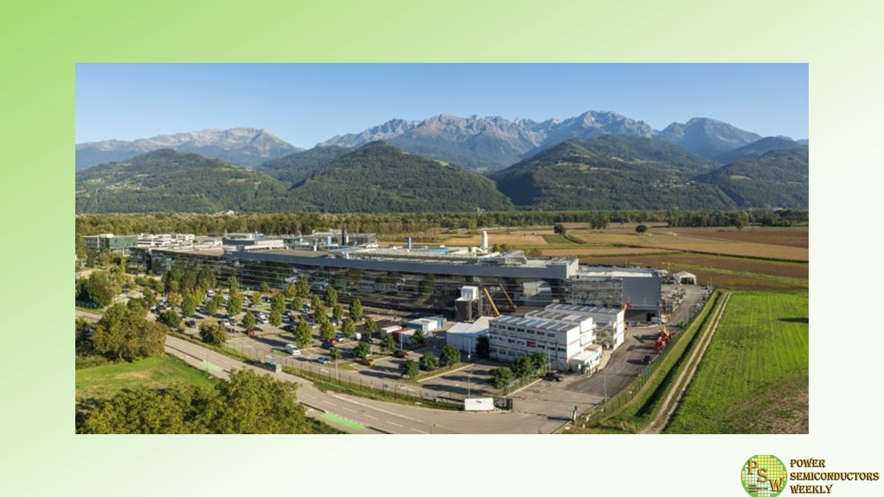
Soitec opened its new plant in Bernin, near Grenoble, in the presence of Thierry Breton, European Commissioner for the Internal Market and Roland Lescure, French Minister Delegate for Industry.
Soitec has developed its SmartSiC™ technology as a response to vehicle electrification challenges.
The technology, based on silicon carbide (SiC), sets a new standard with improved efficiency for energy conversion systems. Thanks to its reduced energy losses, better thermal management and improved power density, the material increases the range and performance of electric vehicles.
Through the application of SmartCut™ technology, each SiC substrate can be used 10 times.
As a result, SmartSiC™ enables electric vehicles to achieve ranges above 500 km, compared with an average 350 km for vehicles using silicon IGBT alternatives – while also reducing CO2 emissions during wafer manufacturing by 70% compared to monocrystalline SiC substrates.
Development of the technology began in 2020 in partnership with CEA-Leti and has received financial support from the French state, the region, local authorities and the European Union.
A new production facility in step with Soitec’s ambition
The new plant will have a 2,500 m2 footprint and a final production capacity of 500,000 SmartSiC™ wafers per year.
It will contribute to Soitec’s strategy of sustainable growth towards a threefold expansion of addressable markets by 2030, reinforcing the company’s leadership position in the strategic semiconductor materials market.
The new plant will lead to the creation of 400 direct jobs, while also reinforcing the attractiveness and dynamism of the “French Silicon Valley” ecosystem.
Pierre Barnabé, Chief Executive Officer of Soitec, stated: “More than ever we are ready to establish our SmartSiC™ technology as a new standard in semiconductor materials for coming generations of electric cars. This plant will enable us to meet growing demand for silicon carbide and achieve a 30% market share by 2030, while helping to make electric mobility more efficient and affordable. Completed in record time, it is the embodiment of our industrial performance and our future-facing strategy, based on the expansion of our product and technology portfolio.
This is also an important day for our region, which is once again showing its dynamic and exemplary approach to industrial innovation, with technologies designed, developed, and manufactured within our ecosystem. We will create jobs and continue to showcase French and European knowhow in global semiconductor markets.”
Original – Soitec
-
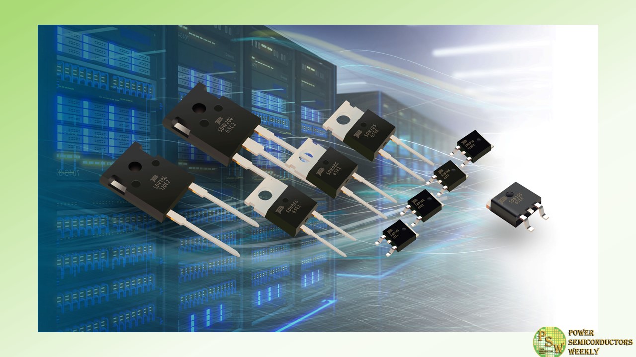
Bourns, Inc. has expanded its 650 and 1200 V Silicon Carbide (SiC) Schottky Barrier Diode (SBD) product family with 10 new models. The 10 new models added to the Bourns® SiC SBD line are designed to address the increasing power density requirements in the latest transportation, renewable energy and industrial systems.
Bourns’ expanded wide band gap diode line delivers the peak forward surge, low forward drop, reduced thermal resistance and low power loss capabilities demanded by today’s high frequency and high current applications. These capabilities also help designers develop smaller, cost-efficient and state-of-the-art power electronics.
As optimal power conversion solutions for DC-DC and AC-DC converters, Switched-Mode Power Supplies (SMPS), photovoltaic inverters, motor drives and other rectification applications, the 10 new models feature currents in the 5-10 A range, with no reverse recovery current to reduce EMI.
This enables them to significantly lower energy losses and further increase efficiency, switching performance and reliability. In addition to providing excellent thermal performance, Bourns’ new SiC SBD models are available in multiple forward voltage, current and package options that include TO220-2, TO247-3, TO252, TO263 and TO247-2.
The 10 new Bourns® BSD SiC SBD models are available now. These models are RoHS compliant, halogen free, Pb free and their epoxy potting compound is flame retardant to the UL 94V-0 standard. For more detailed product information, please see: www.bourns.com/products/diodes/silicon-carbide-sic-schottky-barrier-diodes.
Original – Bourns
-
During the past decade combination “silicon carbide” or more often “SiC” has become very popular in the world of power electronics. Many companies have started to evaluate the possibility of using SiC instead of Si in their projects. As many say, silicon carbide is here to replace silicon, and they might be right considering that SiC MOSFETs used in power semiconductor devices bring numerous advantages compared with their silicon counterparts.
SiC has a higher critical breakdown field and thermal conductivity and, a wider bandgap, which leads to lower energy losses, a lower leakage current at higher temperatures. Besides, SiC can operate at much higher frequencies. On a system level, it means using less additional components, better thermal management, and an overall smaller footprint.
This is one of the reasons why today automotive Tier-1 and OEM companies prefer to use SiC for their new projects in vehicle electrification. With SiC they can get the same efficiency with several times smaller package. For the electric car size and weight of power electronics systems are critical.
Working in the power semiconductors industry for many years, with Si and SiC power devices in particular, I see that the number of companies and end applications adopting silicon carbide is growing fast. Even though SiC is quite a young technology, and the first commercial SiC power MOSFET dates back to 2011, nowadays, we already have over ten SiC power device vendors who deliver high-quality products used in electric vehicles, solar inverters, public transportation, welding equipment, marine, medical and aerospace.
With the number of new SiC fabs and production expansions announced during the past three years it is clear that silicon carbide technology is here to stay, and here to grow further. Many analytical agencies predict that the total SiC market will reach 10 billion USD by 2030 or even earlier. And despite the fact that in volume SiC power semiconductors market still lags behind silicon. It grows faster, quite faster than expected several years ago.
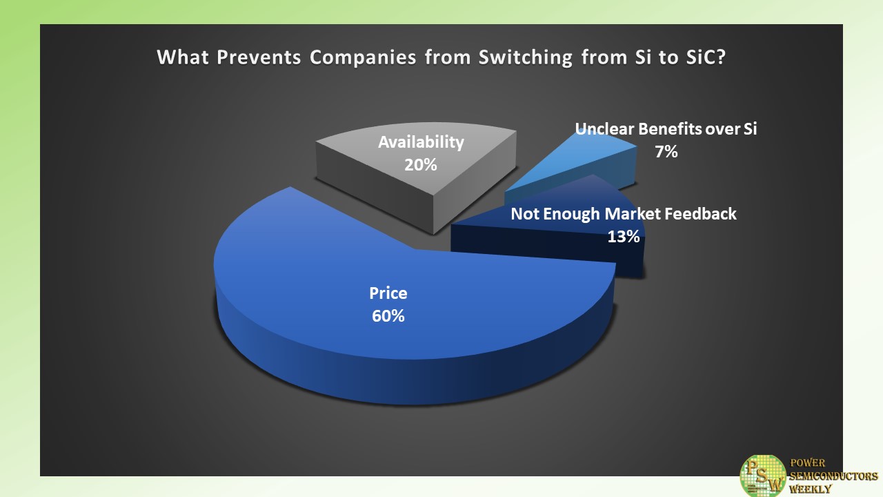
Despite the fast growth and penetration into the power electronics market, many companies still feel uncomfortable when they hear about silicon carbide and the benefits it has. During numerous negotiations and talks with the companies using power semiconductor devices, I shortlisted the most common barriers preventing them from switching from silicon to silicon carbide, or from increasing the number of SiC-based projects they already have.
To further scale this data, recently I had a poll on LinkedIn within the power electronics community. A similar poll I ran during the latest EPE’23 ECCE Europe Conference, which was held in Aalborg, Denmark. Both polls’ participants come from power semiconductors companies or from companies using power semiconductors.
Combined poll results look like this:
- Price – 60%
- Availability – 20%
- Unclear benefits over Si – 7%
- Not enough market feedback – 13%
It is clear that price is still the major concern and barrier. Even though the price has tremendously decreased during the past ten years, it remains one of the key factors why many companies prefer to use Si-based semiconductors.
The availability of SiC wafers or SiC-based devices accounts for another 20% of doubts coming from the end users. The lead time of SiC has been discussed many times, and the situation for many stays unclear. And it is the same for the remaining 20% of poll results coming from unclear benefits of SiC and lack of market feedback. Silicon power devices have been in use for decades, while SiC is just at the beginning of its road. That is why many engineers prefer to work with the technology they know, the technology they have been very familiar with since their school.
From the first look the answers and results of the poll seem to be right and they correspond to the current market situation. However, working with Si and SiC, I know that each and every one of the answers listed are just the barriers and not the final verdict.
Semiconductor companies should pay more attention to those 20% of the answers referring to lack of market data. With the right approach SiC will bring the power semiconductors industry to a new level.
-
Power semiconductors based on silicon carbide (SiC) offer several advantages, like high efficiency, power density, voltage resistance, and reliability. This creates opportunities for new applications and improved charging station technology innovations. Infineon Technologies announced a collaboration with Infypower, a Chinese market leader in new energy vehicle charging. Infineon will provide INFY with the industry-leading 1200 V CoolSiC™ MOSFET power semiconductor devices to improve the efficiency of electric vehicle charging stations.
“The collaboration between Infineon and Infypower in the field of charging solutions for electric vehicles (EV) provides an excellent system-level technology solution for the local EV charging station industry,” said Dr. Peter Wawer, Division President of Infineon’s Green Industrial Power Division. “It will significantly improve charging efficiency, accelerate charging speed, and create a better user experience for owners of electric cars.”
“With Infineon’s more than 20 years of continuous advancement in SiC product offering and the strength of integrated technology, Infypower can consolidate and maintain its technological outstanding position in the industry by adopting state-of-the-art product processes and design solutions“, said Qiu Tianquan, President of Infypower China. “We can also set a new standard for charging efficiency of DC chargers for new energy vehicles. As a result, customers can enjoy more convenience and unique value, promoting the healthy development of the EV charging industry.”
SiC’s high power density enables the development of high-performance, lightweight, and compact chargers, especially for supercharging stations and ultra-compact wall-mounted DC charging stations. Compared to traditional silicon-based solutions, SiC technology in EV charging stations can increase efficiency by 1 percent, reducing energy losses and operating costs. In a 100 kW charging station, this translates to 1 kWh of electricity savings, saving 270 Euros annually and reducing carbon emissions by 3.5 tons. This drives the increasing adoption of SiC power devices in EV charging modules.
As one of the first SiC power semiconductor manufacturers to use trench gate technology for transistors, Infineon has introduced an advanced design that provides high reliability for chargers. The devices offer a high threshold voltage and simplified gate driving . The CoolSiC MOSFET technology has been subjected to marathon stress tests and gate voltage jump stress tests before commercial release and regularly afterwards in form of monitoring to ensure highest gate reliability.
By integrating Infineon’s 1200 V CoolSiC MOSFETs, Infypower’s 30 kW DC charging module offers a wide constant power range, high power density, minimal electromagnetic radiation and interference, high protection performance and high reliability. In this way, it is well suited for the fast charging demand of most EVs while possessing a higher efficiency of 1 percent compared with other solutions on the market. Consequently, significant energy savings and carbon dioxide emission reduction are achieved, which are leading at a global level.
Original – Infineon Technologies
