-

Power Master Semiconductor has released a new package portfolio, TO leadless (TOLL) package for 650V eSiC MOSFET series to meet the increasing demands for high power density and efficiency with superior switching performance in various applications such as AI data center servers, telecom infrastructure, flat panel display power, ESS, and battery formations.
Recently, the rapid growth of artificial intelligence (AI) is expected to drive continued strong data center demand. AI datacenters rely on GPUs that consume 10 to 15 times more power than traditional CPUs. SiC MOSFETs in TOLL package are an optimal solution for the rapidly expanding AI applications today.
The TOLL package has a footprint of 9.9mm x 11.7mm, reducing the PCB area by 30% compared to the D2PAK 7-lead package. Moreover, with a thickness of 2.3mm, it has 60% less height than the D2PAK 7-lead package.
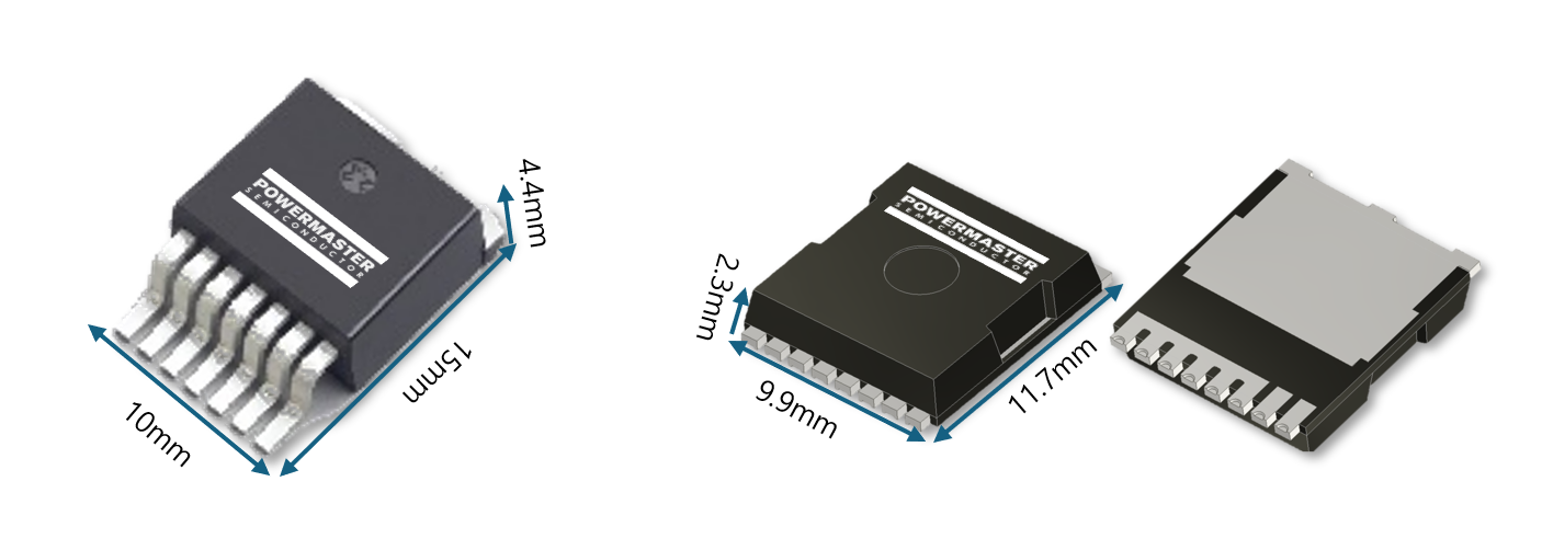
The TOLL offers superior thermal performance and low package inductance (2nH) compared to D2PAK 7-lead package. Kelvin source configuration lowers gate noise and reduces turn-on loss by 60% compared to same device without Kelvin source configuration, enabling higher frequency operation and improved power density. The new PCT65N27M1 has a VDSS rating of 650 V with a typical RDS(ON) of 27mΩ and a maximum drain current (ID) of 84 A.
Power Master Semiconductor’s products in TOLL package has special grooves in the gate and source pins to enhance the performance of the solder joint and offers Moisture Sensitivity Level 1 (MSL 1).
Original – Power Master Semiconductor
-

ROHM announced the adoption of power modules equipped with 4th generation SiC MOSFET bare chips for the traction inverters in three models of ZEEKR EV brand from Zhejiang Geely Holding Group (Geely), a top 10 global automaker. Since 2023, these power modules have been mass produced and shipped from HAIMOSIC (SHANGHAI) Co., Ltd. – a joint venture between ROHM and Zhenghai Group Co., Ltd. to Viridi E-Mobility Technology (Ningbo) Co., Ltd, a Tier 1 manufacturer under Geely.
Geely and ROHM have been collaborating since 2018, beginning with technical exchanges, then later forming a strategic partnership focused on SiC power devices in 2021. This led to the integration of ROHM’s SiC MOSFETs into the traction inverters of three models: the ZEEKR X, 009, and 001. In each of these EVs, ROHM’s power solutions centered on SiC MOSFETs play a key role in extending the cruising range and enhancing overall performance.
ROHM is committed to advancing SiC technology, with plans to launch 5th generation SiC MOSFETs in 2025 while accelerating market introduction of 6th and 7th generation devices. What’s more, by offering SiC in various forms, including bare chips, discrete components, and modules, ROHM is able to promote the widespread adoption of SiC technology, contributing to the creation of a sustainable society.
Original – ROHM
-

onsemi released the newest generation silicon and silicon carbide hybrid Power Integrated Modules (PIMs) in an F5BP package, ideally suited to boost the power output of utility-scale solar string inverters or energy storage system (ESS) applications. Compared to previous generations, the modules offer increased power density and higher efficiencies within the same footprint to increase the total system power of a solar inverter from 300kW up to 350kW.
This means a one-gigawatt (GW) capacity utility-scale solar farm using the latest generation modules can achieve an energy savings of nearly two megawatts (MW) per hour or the equivalent of powering more than 700 homes per year. Additionally, fewer modules are required to achieve the same power threshold as the previous generation, which can reduce power device component costs by more than 25%.
With solar power having achieved the lowest levelized cost of energy (LCOE), it is increasingly becoming the go-to source for renewable power generation around the world. To compensate for solar power’s variability, utility operators are also adding large-scale battery energy storage systems (BESS) to ensure a stable energy flow to the grid. To support this combination of systems, manufacturers and utilities require solutions that offer maximum efficiency and reliable power conversion. Every 0.1% of efficiency improvement can equate to a quarter of a million dollars in annual operational savings for every one gigawatt of installed capacity.
“As a variable energy source dependent on sunlight, continual advances in increasing system efficiencies, reliability and advanced storage solutions are needed to be able to maintain the stability and reliability of global grids during peak and off-peak power demand,” said Sravan Vanaparthy, vice president, Industrial Power Division, Power Solutions Group, onsemi. “A more efficient infrastructure increases adoption and assures us that, as more solar power generation is built out, less energy is wasted and pushes us forward on a path away from fossil fuels.”
The F5BP-PIMs are integrated with 1050V FS7 IGBT and the 1200V D3 EliteSiC diode to form a foundation that facilitates high voltage and high current power conversion while reducing power dissipation and increasing reliability. The FS7 IGBTs offer low turn-off losses and reduce switching losses by up to 8%, while the EliteSiC diodes provide superior switching performance and lower voltage flicker by 15% compared to previous generations.
These PIMs employ an innovative I-type Neutral Point Clamp (INPC) for the inverter module and a flying capacitor topology for the boost module. The modules also use an optimized electrical layout and advanced Direct Bonded Copper (DBC) substrates to reduce stray inductance and thermal resistance. In addition, a copper baseplate further decreases thermal resistance to the heat sink by 9.3%, ensuring the module remains cool under high operational loads. This thermal management is crucial in maintaining the efficiency and longevity of the modules, making them highly effective for demanding applications that require reliable and sustained power delivery.
Original – onsemi
-
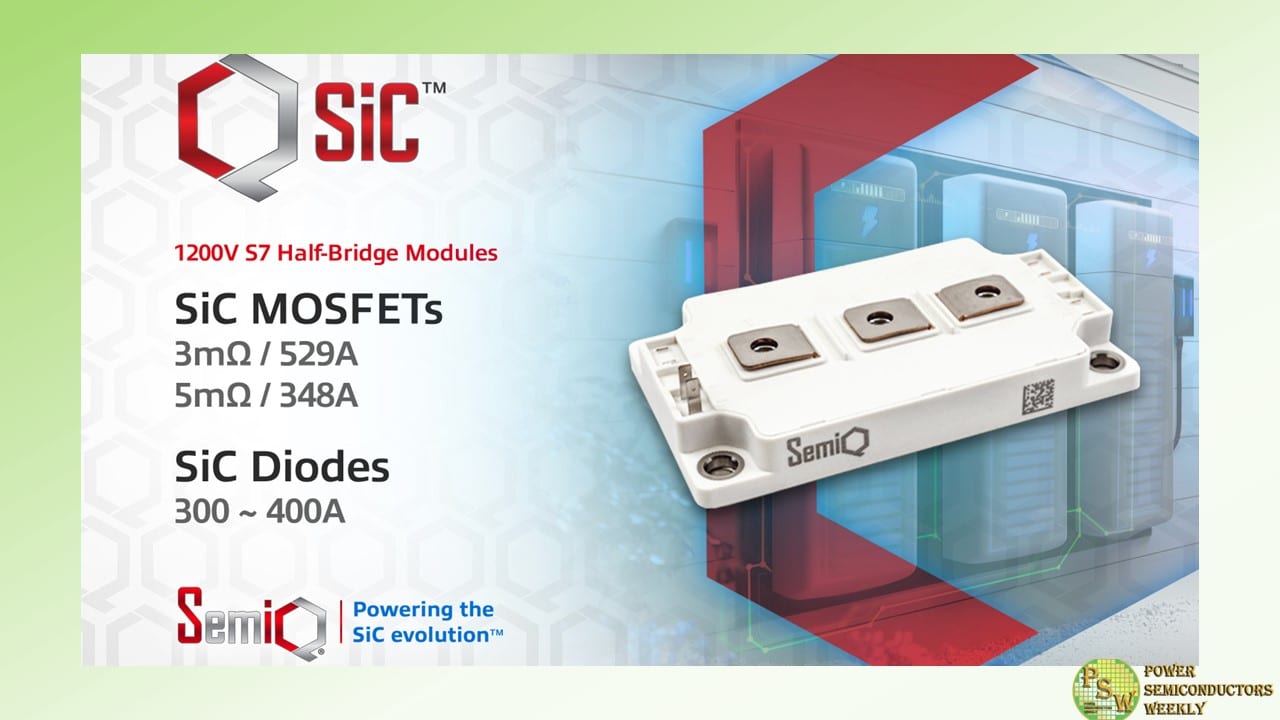
SemiQ Inc announced the addition of an S7 package to its QSiC™ family of 1200V, half-bridge MOSFET and Schottky diode SiC power modules. The parts further enhance design flexibility for power engineers by providing compact, high-efficiency, high-performance options for new designs while supporting drop-in-replacement in legacy systems that require more efficient operation.
This latest announcement sees the availability of a 529A MOSFET module (GCMX003A120S7B1), a 348A MOSFET module (GCMX005A120S7B1), and two low-noise SiC Schottky diode half-bridge modules (GHXS300A120S7D5 and GHXS400A120S7D5) in an S7 package with industry-standard 62.0mm footprints and a height of just 17.0mm.
The new package addresses the size, weight and power requirements of demanding applications ranging from induction heaters, welding equipment and uninterruptible power supplies (UPS) to photovoltaic and wind inverters, energy storage systems, high-voltage DC-DC converters and battery charging systems for electric vehicles (EVs). As well as the compact form factor of the modules themselves, high-efficiency, low-loss operation helps to reduce system heat dissipation and supports the use of smaller heatsinks.
“Our aim is to provide a comprehensive portfolio of SiC technologies that allow designers to optimize the efficiency, performance and size of today’s demanding applications,” says Dr. Timothy Han, President at SemiQ. “Adding new package option to our 1200V QSiC MOSFET and SiC diode module families further extends the choices available to designers who need to create completely new applications or who are looking to upgrade legacy systems without significant redesign.”
Crafted from high-performance ceramics, SemiQ’s modules achieve exceptional performance levels and support increased power density and more compact designs – especially in high-frequency and high-power environments.
To guarantee a stable gate threshold voltage and premium gate oxide quality for each module, SemiQ conducts gate burn-in testing at the wafer level. In addition to the burn-in test, which contributes to mitigating extrinsic failure rates, various stress tests – including gate stress, high-temperature reverse bias (HTRB) drain stress, and high humidity, high voltage, high temperature (H3TRB) – are employed to attain the necessary automotive and industrial grade quality standards. All parts have undergone testing surpassing 1400V.
Part numbers of SemiQ’s new 1200V modules in S7 packages are shown below.
Part Numbers Circuit Configuration Ratings, Packages RdsOn mΩ GCMX003A120S7B1 S7 Half-bridge 1200V/529A, B1 3.0 GCMX005A120S7B1 S7 Half-bridge 1200V/348A, B1 4.9 GHXS300A120S7D5 S7 Half-bridge 1200V/300A, D5 GHXS400A120S7D5 S7 Half-bridge 1200V/400A, D5 Original – SemiQ
-
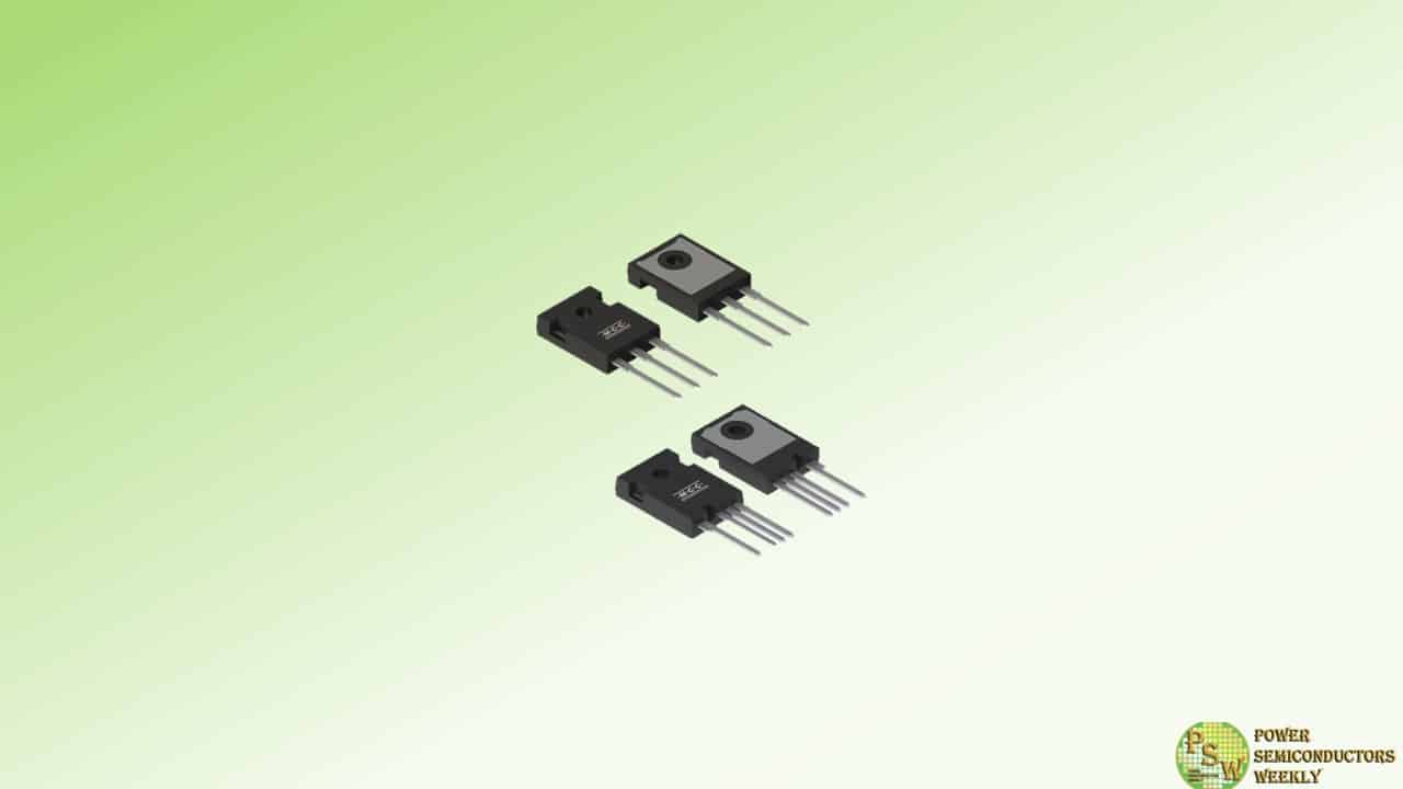
MCC Semi is expanding advanced silicon carbide portfolio with six new 650V SiC MOSFETs. Designed for demanding applications, these components boast high-voltage capability and an on-resistance range of 25 mΩ to 100 mΩ. They’re also equipped with avalanche ruggedness, low switching losses, and enable high-speed switching with a low gate charge.
Their efficiency-boosting design and TO247 package deliver superior thermal performance, while the 3-pin or 4-pin (Kelvin-source pin) options enhance their versatility. These new MOSFETs minimize losses without compromising power handling, making them an intelligent choice for various industrial and telecommunications systems.
Features & Benefits:
- High switching speed with low gate charge
- Low switching losses
- Wide on-resistance selection ranging from 25 mΩ to 100 mΩ
- Avalanche ruggedness for enhanced durability
- TO247 3-pin and 4-pin package options
- Kelvin-source connection for precision (4-pin only)
Original – Micro Commercial Components
-

As global decarbonization efforts drive demand for power semiconductors, Infineon Technologies AG has officially opened the first phase of a new fab in Malaysia that will become the world’s largest and most competitive 200-millimeter silicon carbide (SiC) power semiconductor fab. Malaysian Prime Minister YAB Dato’ Seri Anwar Ibrahim and Chief Minister of the state of Kedah YAB Dato’ Seri Haji Muhammad Sanusi Haji Mohd Nor joined Infineon CEO Jochen Hanebeck, to symbolically launch production.
The highly efficient 200-millimeter SiC power fab will strengthen Infineon’s role as the global leader in power semiconductors. The first phase of the fab, with an investment volume of two billion euros, will focus on the production of silicon carbide power semiconductors and will include gallium nitride (GaN) epitaxy. SiC semiconductors have revolutionized high-power applications because they switch electricity even more efficiently and enable even smaller designs.
SiC semiconductors increase efficiency in electric vehicles, fast charging stations and trains as well as renewable energy systems and AI data centers. 900 high-value jobs will be created already in the first phase. The second phase, with an investment of up to five billion euros, will create the world’s largest and most efficient 200-millimeter SiC power fab. Overall, up to 4.000 jobs will be created with the project.
“New generations of power semiconductors based on innovative technology such as silicon carbide are an absolute prerequisite to achieving decarbonization and climate protection. Our technology increases the energy efficiency of ubiquitous applications such as electric cars, solar and wind power systems and AI data centers. We are therefore investing in the largest and most efficient high-tech SiC production facility in Malaysia, backed by strong customer commitments,” said Jochen Hanebeck, CEO of Infineon Technologies AG. “Since the demand for semiconductors will constantly rise, the investment in Kulim is highly attractive to our customers, who are backing it with their prepayments. It also increases the resilience of the supply chain for critical components needed for the green transition.”
“Infineon’s remarkable project reinforces Malaysia’s position as a rising major global semiconductor hub” says Malaysian Prime Minister YAB Dato’ Seri Anwar Ibrahim. “This major investment, which will locate the world’s largest and most competitive SiC power fab on our shores, will create jobs and opportunities, as well as attract suppliers, universities and top talent. Moreover, it will support Malaysia’s efforts to protect our climate by boosting electrification and increasing the efficiency of many applications, including electric cars and renewable energy. Thus, technology made in Malaysia will become a central part of global decarbonization efforts in the future.”
“Infineon’s deeply rooted presence in Kulim is a testament to the region’s potential as a hub for high-tech industries,” says Kedah Chief Minister YAB Muhammad Sanusi Md Nor. “This investment will not only create high-value job opportunities for the local community, it will also catalyze economic growth in the region. We are committed to continue providing top business conditions in Kedah and supporting Infineon’s efforts to establish a leading semiconductor facility in Kulim, which will have a positive ripple effect on the entire ecosystem.”
Infineon has secured design wins with a total value of approximately five billion euros and has received approximately one billion euros in prepayments from existing and new customers for the ongoing expansion of the Kulim 3 fab. Notably, these design wins include six OEMs in the automotive sector as well as customers in the renewable energy and industrial segments.
Kulim 3 will be closely connected to the Infineon site in Villach, Austria, Infineon’s global competence center for power semiconductors. Infineon already increased capacity for SiC and GaN power semiconductors in Villach in 2023. As “One Virtual Fab” for wide-bandgap technologies, both manufacturing sites now share technologies and processes which allow for fast ramping and smooth and highly efficient operation. The project also offers a high grade of resilience and flexibility, which will ultimately benefit Infineon’s customers.
The expansion will benefit from the excellent economies of scale already achieved for 200-millimeter manufacturing in Kulim. It will complement Infineon’s leading position in silicon, based on 300-millimeter manufacturing in Villach and Dresden. Thus, Infineon is strengthening its technological leadership across the entire spectrum of power semiconductors, in silicon as well as SiC and GaN.
In addition, the investment in wide-bandgap capacity in Kulim strengthens the local ecosystem and proves that Infineon is a reliable partner within the growing semiconductor hub Malaysia. Infineon’s operations in Malaysia started as early as 1973 in Melaka. In 2006, the company opened Asia’s first frontend fab in Kulim. Currently, Infineon employs more than 16.000 highly skilled people in Malaysia.
The Kulim 3 fab will be powered by 100% green electricity and will employ the latest energy efficiency measures to support Infineon’s goal of carbon neutrality. To avoid emissions, Infineon will use a state-of-the-art abatement system and green refrigerants that combine high efficiency with extremely low global warming potential. Other measures to ensure sustainable operations include state-of-the-art recycling of indirect materials and state-of-the-art water efficiency and recycling processes. Infineon is working towards recognition with the renowned Green Building Index certification.
Original – Infineon Technologies
-

Solitron Devices released the SD11740 , 1200V Silicon Carbide (SiC), low RDS(on) MOSFET.
Complimenting a strong offering of high voltage MOSFETs for high reliability/military applications Solitron is expanding its silicon carbide product offering for demanding commercial and industrial applications. Packaged in a SOT-227 the SD11740 offers ultra-low RDS(on) of 8.6mΩ.
The addition of the SOT-227 style package enables higher power applications for Solitron’s SiC based products in EV, power controllers, motor drive, induction heating, solid state circuit breakers and high voltage power supplies. The SD11740 offers 120A of continuous drain current. The SOT-227 features 3kV isolation to a copper heat sink base for outstanding low thermal impedance. The device provides a real Kelvin gate connection for optimal gate control. Either emitter terminal can be used as main or Kelvin emitter.
Designed for use as a power semiconductor switch the SD11740 outperforms silicon based MOSFETs and IGBTs. The standard gate drive characteristics allow for a true drop-in replacement to silicon IGBTS and MOSFETs with far superior performance. Ultra-low gate charge and exceptional reverse recovery characteristics, make them ideal for switching inductive loads and any application requiring standard gate drive.
Original – Solitron Devices
-
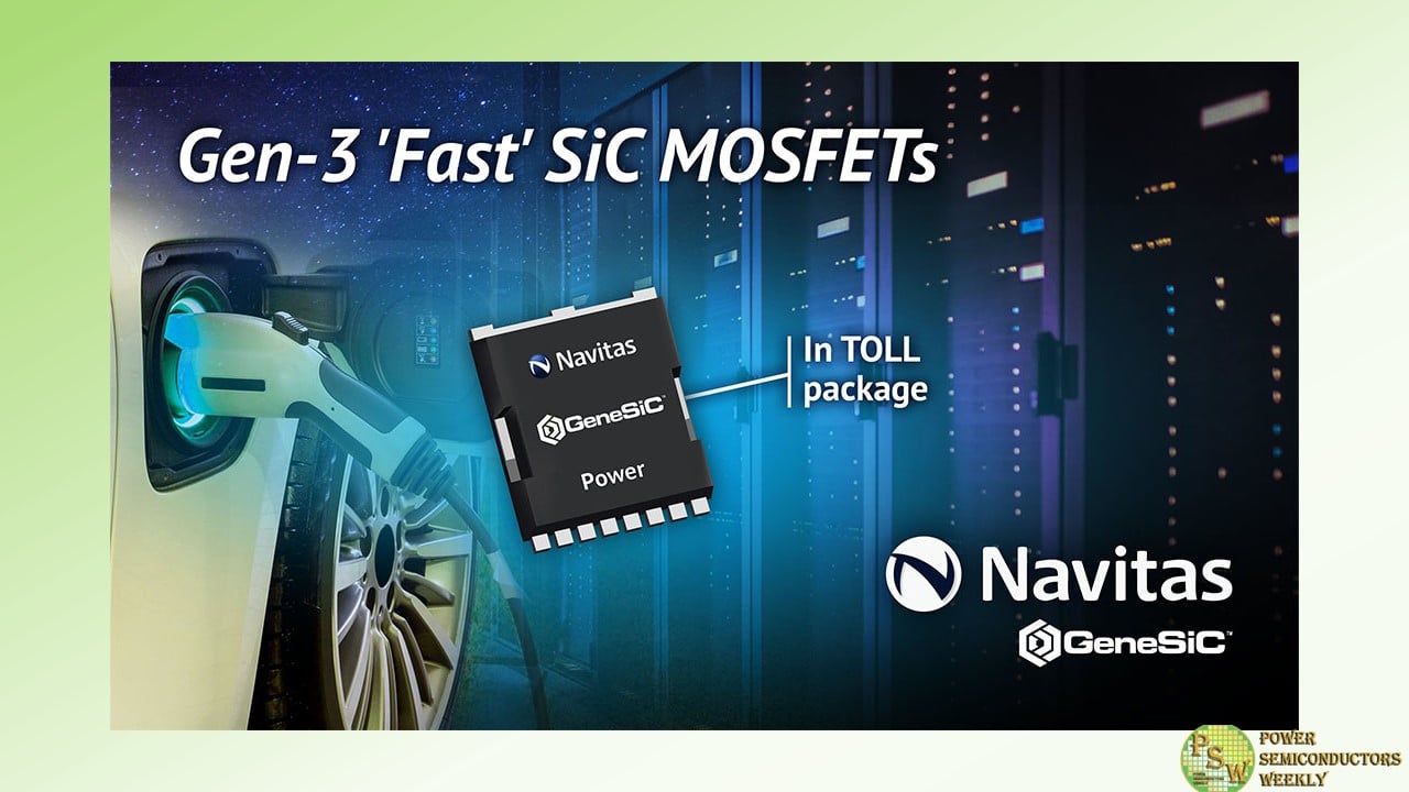
Navitas Semiconductor extended its new portfolio of Gen-3 ‘Fast’ (G3F) 650 V SiC MOSFETs into a thermally-enhanced, rugged, high-speed, surface-mount TOLL (Transistor Outline Leadless) package designed for demanding, high-power, high-reliability applications.
Combining high-power capability and best-in-class low on-resistance of 20 to 55 mΩ, these 650 V SiC MOSFETs have been optimized for the fastest switching speed, highest efficiency, and increased power density demanded by applications such as AI data center power supplies, EV charging and energy storage and solar solutions (ESS).
Navitas’ GeneSiC products use a proprietary ‘trench-assisted planar’ technology that provides world-leading efficiency performance over the temperature range, with G3F MOSFETs delivering high-speed, cool-running performance that ensures up to 25°C lower case temperatures and up to 3x longer life than alternative SiC products.
Navitas’ latest 4.5 kW AI power system reference design features the G3F45MT60L (650V 40 mΩ, TOLL) G3F SiC MOSFET in an interleaved CCM-TP PFC topology. Complemented by the NV6515 (650V, 35mΩ, TOLL) GaNSafe™ Power IC in the LLC stage, the 4.5 kW solution has a peak efficiency above 97% and, at 137 W/inch3, it is the world’s highest power density AI PSU. For 400 V-rated EV battery systems, G3F in TOLL is an ideal technology for on-board chargers (OBC), DC-DC converters, and traction drives ranging from 6.6 to 22 kW.
The surface-mount TOLL package offers a 9% reduction in junction-to-case thermal resistance (RTH,J-C), 30% smaller PCB footprint, 50% lower height, and 60% smaller size than the traditional D2PAK-7L, enabling highest-power-density solutions, as demonstrated in the 4.5 kW AI solution. Additionally, with a minimal package inductance of only 2 nH, excellent fast-switching performance and lowest dynamic losses are achieved.
The G3F family in TOLL package is released and available for purchase.
Original – Navitas Semiconductor
-

Toshiba Electronic Devices & Storage Corporation and Toshiba Corporation (Toshiba Group) have developed technology that mitigates the parasitic oscillation that occurs during switching operations by power modules with silicon carbide (SiC) MOSFETs connected in parallel, even with a 60% smaller gate resistance than is typical. The technology reduces power loss in power modules, mitigates oscillation, and realizes highly reliable switching operations.
The drive for carbon neutrality is stimulating demand for technologies that improve energy efficiency in many areas, including renewables, railways, and industrial equipment. In these sectors, the application of power modules built around SiC MOSFETs is seen as a solution that supports high-speed switching at high voltages and large currents—which is particularly important for the miniaturization of power converters, where higher switching frequencies result in higher rates of switching losses against power consumption.
Connecting multiple chips in parallel in power modules can form oscillation circuits, the result of wiring inductance between the chips and their parasitic capacitance. It can reduce module reliability if not countered, which is usually done by increasing gate resistance. However, this approach slows switching speed, resulting in a trade-off with switching losses. For power modules with SiC MOSFETs to perform high-speed switching, another approach is needed.
Toshiba Group used an equivalent circuit model of the power module (Figure 1) to determine the theoretical condition that triggers parasitic oscillation, and developed a wiring layout less likely to cause it. This was done by analyzing simulations of parasitic oscillation occurs when Lg/Ls, the ratio of gate-to-gate inductance Lg and source-to-source inductance Ls of parallel chips, is below a certain value (Figure 2). As increasing Lg/Ls is an effective means of mitigating parasitic oscillation, Toshiba Group fabricated prototype modules with different Lg/Ls and measured switching. This confirmed that increasing Lg/Ls mitigated oscillation, even with a 60% smaller gate resistance than that required by the alternative approach of increasing gate resistance (Figure 3).
Applying this approach to oscillation mitigation in power modules now under development has realized a power module less likely to cause parasitic oscillation, even with minimal gate resistance, that achieves low power loss with mitigated oscillation, and delivers highly reliable switching operation. Toshiba Group will continue to make refine the modules toward an early product launch.
Toshiba Group presented the details of this technology on June 6 at the 36th International Symposium on Power Semiconductor Devices and ICs (ISPSD) 2024, an international power semiconductor conference held in Bremen, Germany from June 2 to 6.
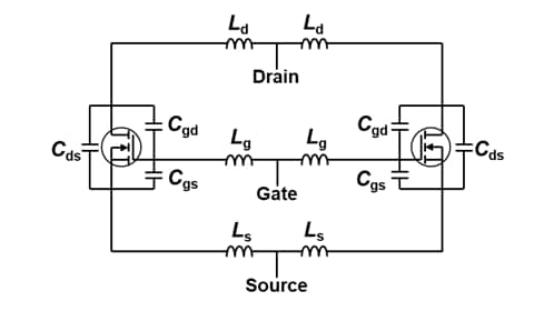
Figure 1. Model equivalent circuit of two MOSFETs connected in parallel 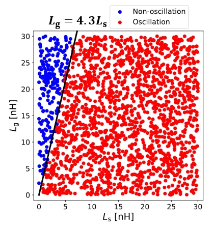
Figure 2. Simulation of oscillation in two MOSFETs with zero gate resistance connected in parallel 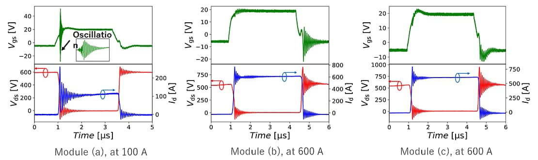
Vgs: Gate-Source voltage, Vds: Drain-Source voltage, Id: Drain current
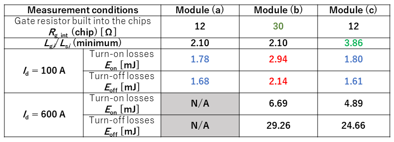
Figure 3. Switching waveforms and switching losses of the prototype modules (Source: Toshiba Group tests) Original – Toshiba
-

MCC introduced the latest additions to its robust portfolio: 10 1200V SiC N-channel MOSFETs in versatile TO-247-4, TO-247-4L, and TO-247AB packages. These new MOSFETs are available in 3-pin and 4-in (Kelvin source) configurations and meet the rising demand for high-power, high-voltage applications.
Boasting exceptional on-resistance values from 21mΩ to 120mΩ (typ.) and fast switching speeds, these components are the ones you can count on for reliable performance. Their excellent thermal properties and fast intrinsic body diode ensure smooth, efficient operation in the most challenging conditions, making them a must-have for critical power systems.
Features & Benefits:
- High-power capability: 1200V MOSFET with SiC technology
- Fast, reliable switching: Intrinsic body diode improves efficiency & ruggedness Enhanced performance: High switching speed with low gate charge
- Wide on-resistance selection: ranging from 21mΩ to 120mΩ (typ.)
- Efficiency: Superior thermal properties and low switching losses
- Durability: Avalanche ruggedness
- Versatility: TO247 3-pin and 4-pin package options
Original – Micro Commercial Components
