-
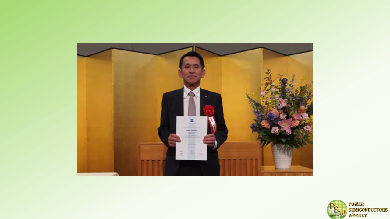
Toshiba Electronic Devices & Storage Corporation announced that Atsushi Tomishima, an Expert at its Electronic Devices & Storage Research & Development (R&D) Center, is a recipient of a 2023 1906 Award from the International Electrotechnical Commission (IEC).
The IEC is the world leader in evaluating and publishing international standards for electrical, electronic, and related technologies. The 1906 Award, created in 2006 and named for the year IEC was founded, honors the work of experts around the world whose work is fundamental to IEC and the execution of its important mission. The Award also recognizes recent and exceptional achievements—a project or other contribution—related to IEC’s activities that contribute in a significant way to advancing the Commission’s work.
Mr. Tomishima, a researcher in the Package Solution Technology Development Dept. at Toshiba’s Electronic Devices & Storage R&D Center, has been an expert member representing Japan on the IEC’s subcommittee on integrated circuit technology (TC47/SC47A) since FY2015. He also serves as an executive member of the electromagnetic compatibility (EMC) subcommittee of the Japan Electronics and Information Technology Industries Association, and has led the subcommittee’s activities, and consolidated numerous opinions and proposals on standardization.
At IEC’s EMC simulation modelling (SC47A WG2) and EMC measurement methods on Integrated circuit (WG9) working groups, he has elicited opinions from many countries, ensured a full understanding of each participant’s position, and summarized discussions.
Through these activities, he received this award in recognition of his significant contribution to the efficient promotion of standardization in the semiconductor design and testing field. These international standards established by Mr. Tomishima’s activities allow us to accurately evaluate the noise characteristics of semiconductors themselves, greatly contributing to improving the quality of product design such as integrated circuits and automobiles.
Toshiba will continue to promote international standardization activities in the electric and electronic technologies areas.
Original – Toshiba
-
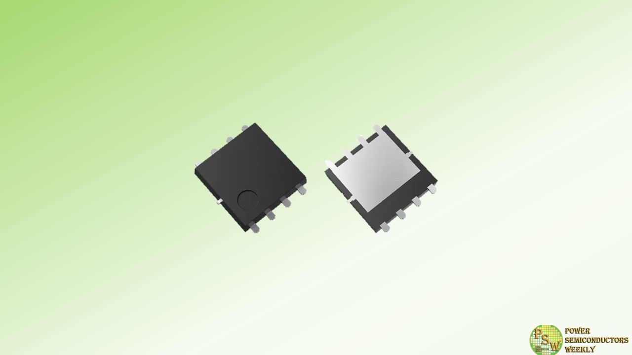
Toshiba Electronic Devices & Storage Corporation has started mass production of three 40 V N-channel MOSFETs using SOP Advance(WF) package for automotive and has expanded its lineup. The three models are “XPHR9904PS, XPH2R404PS and XPH3R304PS.”
The new products reduce drain-source On-resistance with the U-MOSIX process as with Toshiba’s precedence release products XPHR7904PS and XPH1R104PS. The drain-source On-resistance of XPH2R404PS is 2.4 mΩ (max), which is approximately 27 % lower than that of Toshiba’s existing product TPCA8083, and XPH3R304PS is 3.3 mΩ (max), which is approximately 42 % lower than that of Toshiba’s existing product TPCA8085.
The drain-source On-resistance of XPHR9904PS is 0.99 mΩ (max). Reducing drain-source On-resistance of these products contributes to low power consumption of automotive equipment. In addition, they are qualified with the automotive reliability standard AEC-Q101. The PPAP of IATF16949 is also available.
The package is a surface mount type SOP Advance(WF) that uses a wettable flank terminal structure, which facilitates automated visual inspection of the board mounting state.
Toshiba’s automotive MOSFETs support a variety of automotive applications and meet a wide range of customer needs.
Applications
- Automotive equipment: motor drives, switching power supplies, load switches, etc.
Features
- Low On-resistance
XPHR9904PS: RDS(ON)=0.99 mΩ (max) (VGS=10 V)
XPH2R404PS: RDS(ON)=2.4 mΩ (max) (VGS=10 V)
XPH3R304PS: RDS(ON)=3.3 mΩ (max) (VGS=10 V) - AEC-Q101 qualified
- PPAP of IATF16949 available
Original – Toshiba
-

Toshiba Electronic Devices & Storage Corporation announced new board of directors, with an effective date of October 1, 2023. The composition of the Board of Directors and the company’s Auditors, as of October 1, 2023, will be as follows.
Directors and Officers of the Company
- Hiroyuki Sato President & CEO (Toshiba Corporation)
- Seiichi Mori
- Norifumi Inukubo (Toshiba Corporation)
- Hiroshi Kuriki (Toshiba Corporation)
- Shin Kurosawa
- Noriyasu Kurihara
- Hiroyuki Shinki (Toshiba Corporation)
- Yutaka Sata (Toshiba Corporation)
Auditors
- Hiroki Okada
- Masami Takaoka
- Akira Nakanishi (Toshiba Corporation)
Retiring Director as of September 30, 2023
- Takeshi Kamebuchi
- Kenji Kishimoto
- Takashi Miyamori
- Shigenao Noda
- Ikuko Shimogawara
Original – Toshiba
-
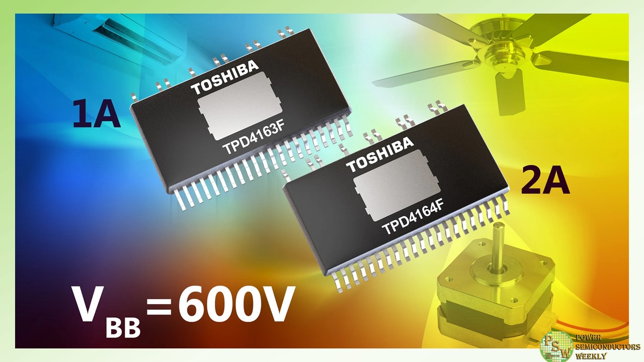
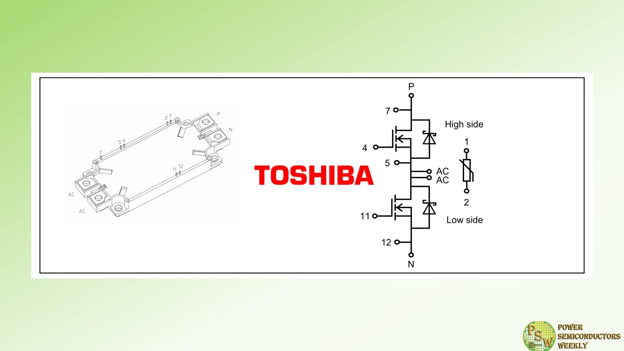
Toshiba Electronics Europe GmbH launched two products for brushless DC (BLDC) motor drive applications including fan motors, ventilation fan, air conditioners, air cleaners, and pumps.
Each of the intelligent power devices (IPD) incorporate 600V-rated IGBTs and a matched gate driver as a one-chip solution in a single compact package. The output DC current (IOUT) rating of the TPD4163F is 1A while the TPD4164F is rated at 2A.
The two devices (TPD4163F and TPD4164F) have an IGBT saturation voltage (VCEsat) of 2.6V and 3.0V respectively, while the Diode forward voltage (VF) is 2.0V and 2.5V.
Both devices are housed in a miniature surface mount HSSOP31 package. With dimensions of just 17.5mm x 11.93mm x 2.2mm, the PCB footprint is reduced by around 63% when compared with Toshiba’s existing DIP26 package products. This makes a significant contribution to reducing the space required for motor drive circuit boards.
In addition, in geographic regions where the power supply is unstable, the supply voltage may fluctuate significantly. Therefore, to improve reliability, the supply voltage rating (VBB)has been increased from 500V to 600V to introduce more design margin.
To support the new devices, Toshiba has developed a reference design for BLDC sensorless brushless DC motor drive utilizing the new TPD4164F and a microcontroller TMPM374FWUG.
Toshiba will continue to expand their product lineup with various packages and improved characteristics, contributing to customers’ design flexibility and carbon neutrality through energy-saving motor control.
Volume production shipments of both new devices (and the reference design board) start today.
Original – Toshiba
-
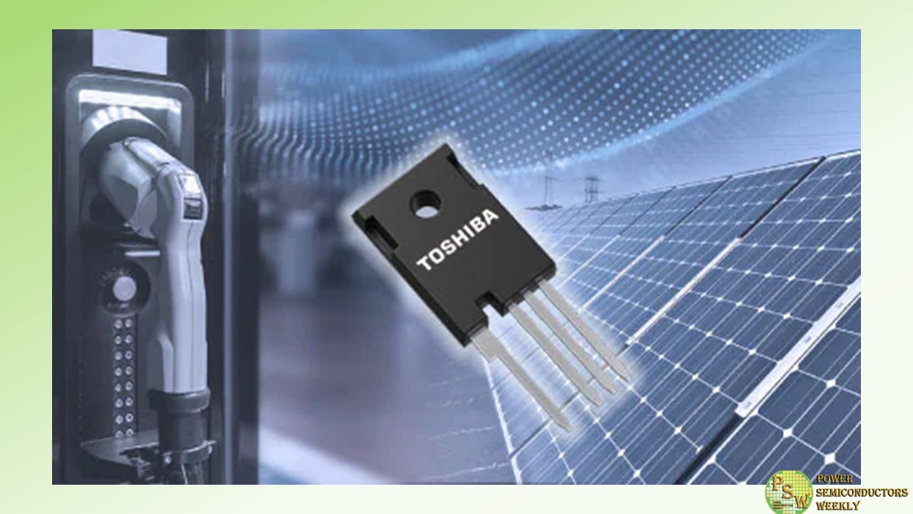
Toshiba Electronic Devices & Storage Corporation has launched silicon carbide (SiC) MOSFETs, the “TWxxxZxxxC series,” that use a four-pin TO-247-4L(X) package that reduces switching loss with the company’s latest 3rd generation SiC MOSFETs chip for industrial equipment. Volume shipments of ten products, five with 650V ratings and five with 1200V, start today.
The new products are the first in Toshiba’s SiC MOSFET line-up to use the four-pin TO-247-4L(X) package, which allows Kelvin connection of the signal source terminal for the gate drive. The package can reduce the effect of source wire inductance inside the package, improving high-speed switching performance. For the new TW045Z120C, the turn-on loss is approximately 40% lower and the turn-off loss reduced by approximately 34%, compared with Toshiba’s current product TW045N120C in a three-pin TO-247 package. This helps to reduce equipment power loss.
Applications
- Switching power supplies (servers, data centers, communications equipment, etc.)
- EV charging stations
- Photovoltaic inverters
- Uninterruptible power supplies (UPS)
Features
- Four-pins TO-247-4L(X) package:
Switching loss is reduced by Kelvin connection of the signal source terminal for the gate drive - 3rd generation SiC MOSFETs
- Low drain-source On-resistance x gate-drain charge
- Low diode forward voltage: VDSF=-1.35V (typ.) (VGS=-5V)
Original – Toshiba
-
Toshiba Electronic Devices & Storage Corporation developed “MG250YD2YMS3,” the industry’s first 2200V dual silicon carbide (SiC) MOSFET module for industrial equipment. The new module has a drain current (DC) rating of 250A and uses the company’s third generation SiC MOSFET chips. It is suitable for applications that use DC1500V, such as photovoltaic power systems and energy storage systems. Volume shipments start today.
Industrial applications like those mentioned above generally use DC1000V or lower power, and their power devices are mostly 1200V or 1700V products. However, anticipating widespread use of DC1500V in coming years, Toshiba has released the industry’s first 2200V product.
MG250YD2YMS3 offers low conduction loss with a low drain-source on-voltage (sense) of 0.7V (typ.). It also offers lower turn-on and turn-off switching loss of 14mJ (typ.) and 11mJ (typ.) respectively, an approximately 90% reduction against a typical silicon (Si) IGBT. These characteristics contribute to higher equipment efficiency. Realizing low switching loss also allows the conventional three-level circuit to be replaced with a two-level circuit with a lower module count, contributing to equipment miniaturization.
Toshiba will continue to meet the market needs for high efficiency and the downsizing of industrial equipment.
Applications
Industrial Equipment
- Renewable energy power generation systems (photovoltaic power systems, etc.)
- Energy storage systems
- Motor control equipment for industrial equipment
- High frequency DC-DC converter, etc.
Features
- Low drain-source on-voltage (sense):
VDS(on)sense=0.7V (typ.) (ID=250A, VGS=+20V, Tch=25°C) - Low turn-on switching loss:
Eon=14mJ (typ.) (VDD=1100V, ID=250A, Tch=150°C) - Low turn-off switching loss:
Eoff=11mJ (typ.) (VDD=1100V, ID=250A, Tch=150°C) - Low stray inductance:
LsPN=12nH (typ.)
Original – Toshiba
-
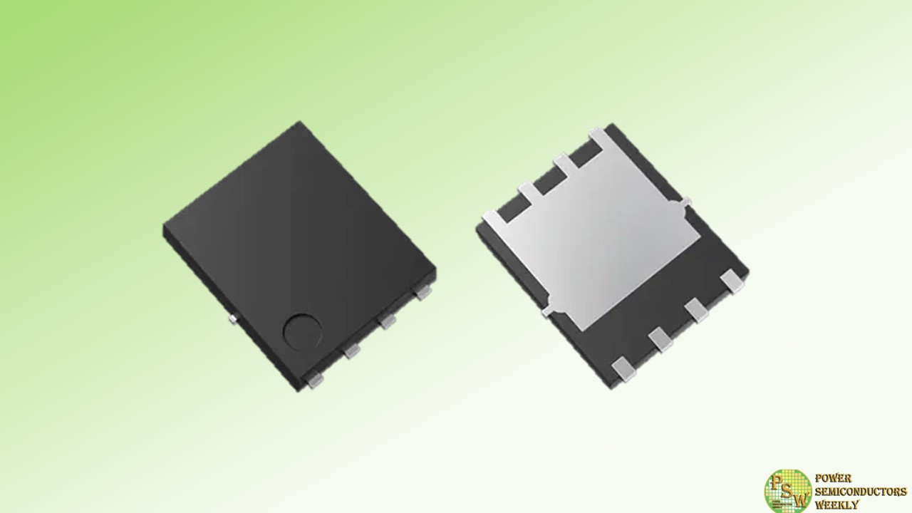
Toshiba Electronic Devices & Storage Corporation has launched three 80 V N-channel power MOSFET products that use its latest generation process “U-MOSX-H series” and are suitable for switching power supplies for industrial equipment—used for such as data centers and communication base stations—and expanded the lineup.
The new products use the surface mount type SOP Advance(N) package, and their drain-source On-resistance (max) is 3 mΩ for “TPH3R008QM”, 6 mΩ for “TPH6R008QM”, and 8.8 mΩ for “TPH8R808QM”.
The new products have reduced the figure of merits (FOMs: expressed as On-resistance × charge characteristics.) In case of TPH3R008QM, it has reduced its FOMs, drain-source On-resistance × total gate charge by approximately 48 %, drain-source On-resistance × gate switch charge by approximately 16 %, and drain-source On-resistance × output charge by approximately 33 %, compared to Toshiba’s existing product TPH4R008NH. This contributes to lowering power consumption of equipment.
Toshiba is expanding its lineup of products to help cut equipment power consumption.
Applications
- Switching power supplies (high efficiency AC-DC converters, high efficiency DC-DC converters, etc.)
- Motor control equipment (motor drives, etc.)
Features
- Latest generation process U-MOSX-H series
- Low On-resistance:
TPH3R008QM RDS(ON)=3 mΩ (max) (VGS=10 V)
TPH6R008QM RDS(ON)=6 mΩ (max) (VGS=10 V)
TPH8R808QM RDS(ON)=8.8 mΩ (max) (VGS=10 V) - High channel temperature: Tch (max)=175 °C
Original – Toshiba
-
Toshiba Electronic Devices & Storage Corporation has launched two automotive 40V N-channel power MOSFETs, “XPJR6604PB” and “XPJ1R004PB,” that use Toshiba’s new S-TOGL™ (Small Transistor Outline Gull-wing Leads) package with U-MOS IX-H process chips. Volume shipments start today.
Safety-critical applications like autonomous driving systems ensure reliability through redundant design, with the result that they integrate more devices and require more mounting space than standard systems. Accordingly, advancing size reductions in automotive equipment requires power MOSFETs that can be mounted at high current densities.
XPJR6604PB and XPJ1R004PB use Toshiba’s new S-TOGL™ package (7.0mm×8.44mm) which features a post-less structure unifying the source connective part and outer leads. A multi-pin structure for the source leads decreases package resistance.
The combination of the S-TOGL™ package and Toshiba’s U-MOS IX-H process achieve a significant On-resistance reduction of 11% against Toshiba’s TO-220SM (W) package product, which has the same thermal resistance characteristics. The new package also cuts the required mounting area by approximately 55% against the TO-220SM(W) package.
On top of this, the 200A drain current rating of the new package is higher than Toshiba’s similarly sized DPAK + package (6.5mm×9.5mm), enabling high current flow. Overall, the S-TOGL™ package realizes high-density and compact layouts, reduces the size of automotive equipment, and contributes to high heat dissipation.
Since automotive equipment is used in extreme temperature environments, the reliability of surface mounting solder joints is a critical consideration. The S-TOGL™ package uses gull-wing leads that reduce mounting stress, improving the reliability of the solder joint.
Assuming that multiple devices will be connected in parallel for applications requiring higher-current operation, Toshiba supports grouping shipment for the new products, in which the gate threshold voltage is used for grouping. This allows designs using product groups with small characteristic variation.
Toshiba will continue to expand its product line-up of power semiconductor products and contribute to the realization of carbon neutrality with more user-friendly, high-performance power devices.
Features:
- New S-TOGL™ package: 7.0mm×8.44mm (typ.)
- Large drain current rating:
XPJR6604PB: ID=200A
XPJ1R004PB: ID=160A - AEC-Q101 qualified
- IATF 16949/PPAP available[4]
- Low On-resistance:
XPJR6604PB: RDS(ON)=0.53mΩ (typ.) (VGS=10V)
XPJ1R004PB: RDS(ON)=0.8mΩ (typ.) (VGS=10V)
Original – Toshiba
-
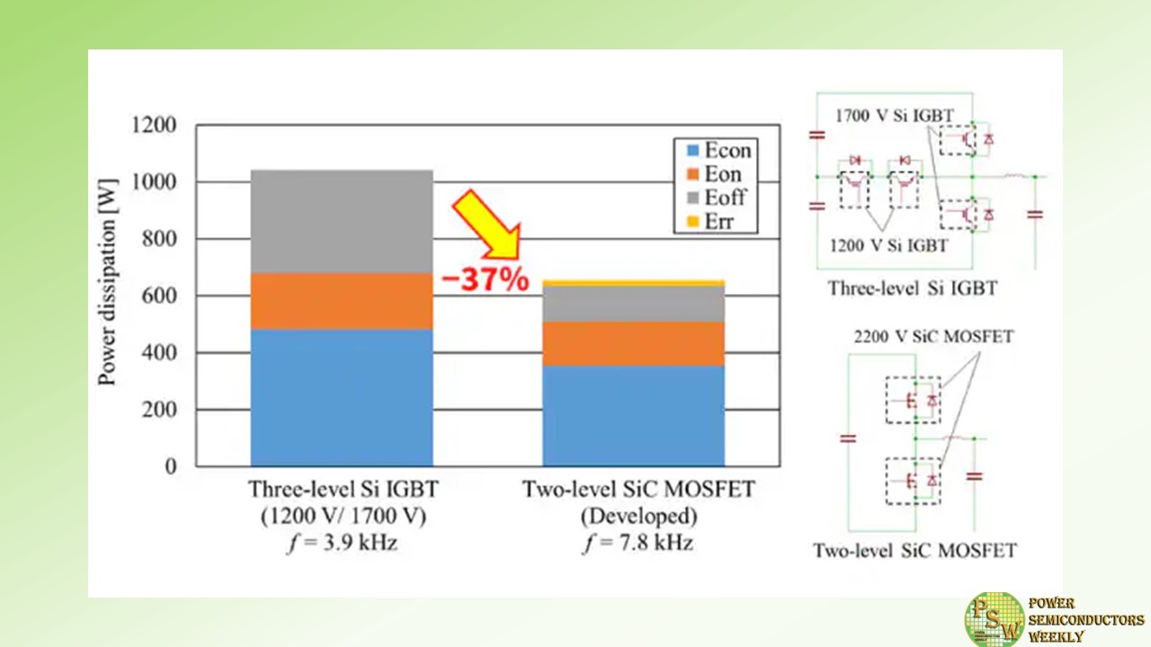
Toshiba Electronic Devices & Storage Corporation has developed 2200 V silicon carbide (SiC) metal oxide semiconductor field effect transistors (MOSFETs) for photovoltaic (PV) inverters. A two-level inverter with the new devices realized higher frequency operation and lower power loss than a conventional three-level silicon (Si) insulated gate bipolar transistor (IGBT) inverter. The new MOSFETs also contribute to simplification of inverter systems and reductions in their size and weight.
Three-level inverters enjoy the advantage of low switching losses because the voltage applied to switching devices in the inverters during off-state is half the line voltage. Against this, two-level inverters have fewer switching modules than three-level inverters, realizing a simpler, smaller, and lighter system. However, they require semiconductors with higher breakdown voltage, as the applied voltage is equal to the line voltage. Also, demand for semiconductors with both low loss and high breakdown voltage is growing as 1500 V DC line voltage systems are introduced in photovoltaic and other renewable energy markets.
Toshiba Electronic Devices & Storage Corporation has developed 2200 V Schottky barrier diode (SBD)-embedded SiC MOSFETs for two-level inverters in 1500 V DC voltage systems. The impurity concentration and thickness of the drift layer has been optimized to maintain the same relationship between the on-resistance and the breakdown voltage as our existing products, and also to achieve high resistance to cosmic rays, a requirement for PV systems. It has also been confirmed that embedding SBDs clamped parasitic PN junctions between the p-base regions and the n-drift layer secure high reliability in reverse conduction.
Switching energy loss for the developed all-SiC module is far lower than for the Si module (Si IGBTs + Si fast recovery diodes) with the same 2000 V rated voltage class. Estimates of inverter power dissipation found that the developed SiC module achieves higher frequency operation twice that of a conventional Si IGBT, as well as a 37% lower loss for the two-level SiC inverter against the three-level Si inverter. The higher frequency operation enables downsizing and weight reduction of other system components, such as heat sinks and filters.
Original – Toshiba
-
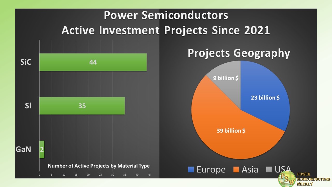
Power semiconductors companies continue to invest heavily in new factories, production capacity expansions, and R&D centers. Thus, recently the total value of the active investment projects launched since 2021 has surpassed 70 billion USD.
Driven by the pandemic and geopolitics, major power semiconductors companies started to invest more in new factories and joint ventures to have more confidence in their own supply chain in the future.
As of today, it is obvious to see the major split of power semiconductors into three geographical regions – the USA, Europe, and Asia. Asia may as well be divided into several regions with China being the leading investor of all.
Despite the ongoing tensions and export restrictions between the US, Europe, and China related to advanced semiconductors, when it comes to power semiconductors European companies continue to invest in the Chinese market expanding their product capacity or establishing new joint ventures like STMicroelectronics and Sanan Optoelectronics did recently.
Even with some delay, Japanese companies like ROHM, Mitsubishi Electric, Fuji Electric, Renesas Electronics, Toshiba, and others, pushed by their US and European competitors, announced their own projects aimed to secure the capacity on the wafer and device level to correspond to the growing demand for Si and SiC based power semiconductors coming from the electric vehicle and charging, photovoltaics, battery energy storage systems, and the other emerging applications.
If we take a closer look at all projects announced, SiC is the leading technology with over 60% of total investment. Over 25 market leaders announced their plans to invest in silicon carbide.
Thus, ROHM is investing in new production to multiply its SiC capacity in the coming years. Mitsubishi Electric teams up with Coherent to scale manufacturing of SiC power devices on a 200 mm SiC technology platform as one of the steps of their 260 billion yen investment project planned till March 2026.
Infineon Technologies continues to bet on both local European and Asian markets investing in their new fab in Dresden and expanding backend operations in Indonesia. STMicroelectronics continues to invest in WBG semiconductors with the ongoing construction of a new wafer fab in Sicily announced in 2022.
With a global total number of new investment projects of over 80, the US companies Wolfspeed, onsemi, and Microchip Technology, similar to their European counterparts, invest locally, in Europe and Asian markets. Totally the US semiconductor companies announced new projects valued at almost 9 billion USD.
With the US and EU Chips Acts, and similar initiatives in China, Japan, South Korea, and some other countries, it is clear that the investment into power semiconductors industry will continue to reach 100 billion USD soon.
