-
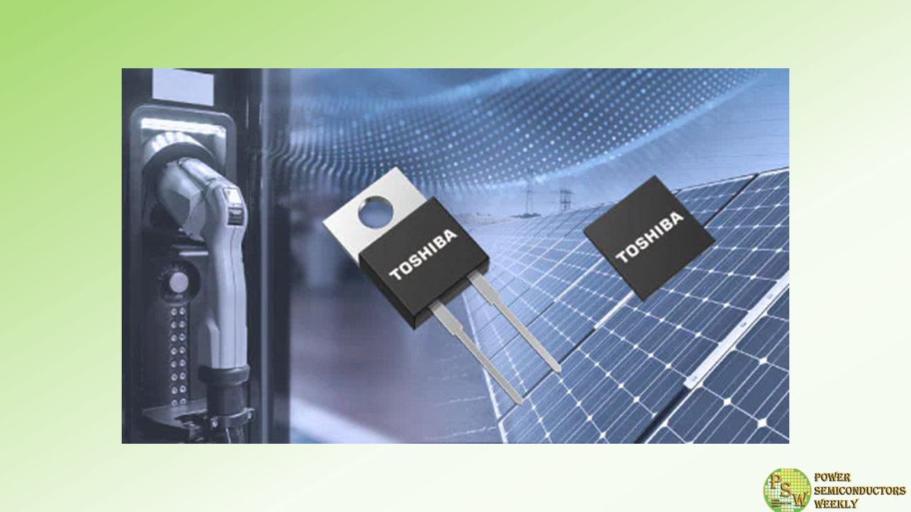
Toshiba Electronic Devices & Storage Corporation has launched the “TRSxxx65H series,” the company’s third and latest generation of silicon carbide (SiC) Schottky barrier diodes (SBDs) for industrial equipment. Volume shipments of the first 12 products, all 650V, start today, with seven products housed in TO-220-2L packages and five in DFN8×8 packages.
The new products use a new metal in a third generation SiC SBD chip that optimizes the junction barrier Schottky (JBS) structure of the second generation products. They achieve industry-leading low forward voltage of 1.2V (Typ.), 17% lower than the 1.45V (Typ.) of the previous generation.
They also improve the trade-offs between forward voltage and total capacitive charge, and between forward voltage and reverse current, which reduces power dissipation and contributes to high efficiency of equipment.
Applications
- Switching power supplies
- EV charging stations
- Photovoltaic inverters
Features
- Industry-leading low forward voltage: VF=1.2V (Typ.) (IF=IF(DC))
- Low reverse current:
TRS6E65H IR=1.1μA (Typ.) (VR=650V) - Low total capacitive charge:
TRS6E65H QC=17nC (Typ.) (VR=400V, f=1MHz)
Original – Toshiba
-
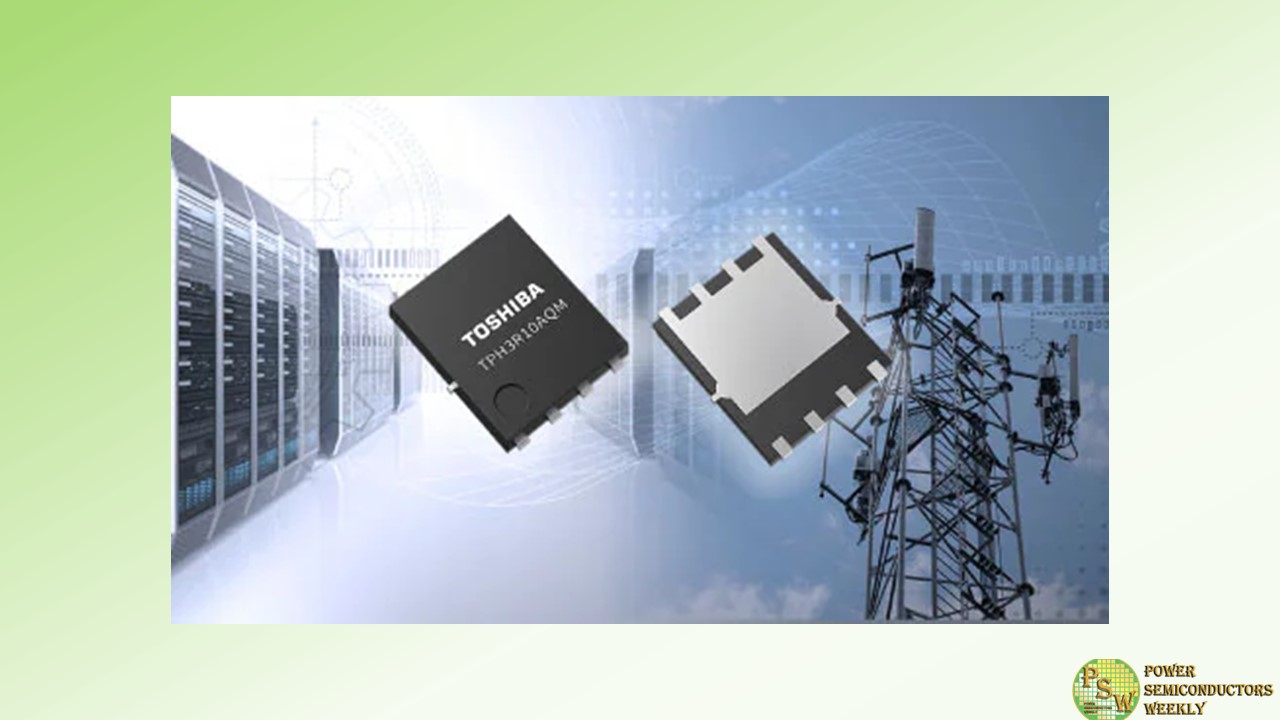
Toshiba Electronic Devices & Storage Corporation (“Toshiba”) has launched “TPH3R10AQM,” a 100V N-channel power MOSFET fabricated with Toshiba’s latest-generation process, U-MOS X-H. The product targets applications such as switching circuits and hot swap circuits on the power lines of industrial equipment used for data centers and communications base stations.
TPH3R10AQM has industry-leading 3.1mΩ maximum drain-source On-resistance, 16% lower than Toshiba’s 100V product, “TPH3R70APL,” which uses the earlier generation process. By the same comparison, TPH3R10AQM has expanded its safe operating area by 76% making it suitable for linear mode operation. Reducing the On-resistance and expanding the linear operating range in the safe operating area reduce the number of parallel connections. Furthermore, its gate threshold voltage range of 2.5V to 3.5V, makes it less likely to malfunction due to gate voltage noise.
The new product uses the highly footprint compatible SOP Advance(N) package.Toshiba will continue to expand its line-up of power MOSFETs that can increase the efficiency of power supplies by reducing loss, and help lower equipment power consumption.
Applications
- Power supplies for communications equipment such as for data centers and communications base stations
- Switching power supplies (High efficiency DC-DC converters, etc.)
Features
- Featuring Industry-leading excellent low On-resistance: RDS(ON)=3.1mΩ (max) (VGS=10V)
- Wide safe operating area
- High channel temperature rating: Tch (max)=175°C
Original – Toshiba
-
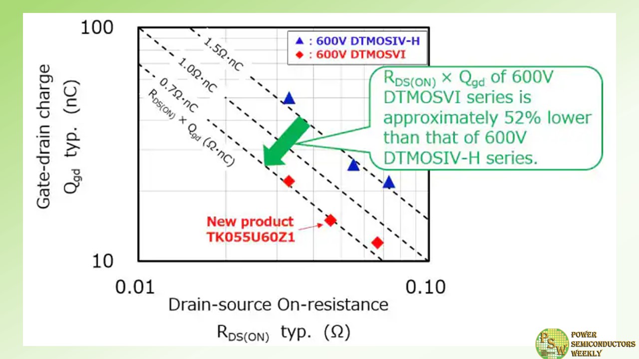
Toshiba Electronic Devices & Storage Corporation (“Toshiba”) has expanded its line-up of N-channel power MOSFETs fabricated with the latest-generation process, with a 600V super junction structure suitable for data centers, switching power supplies, and power conditioners for photovoltaic generators. The new product, “TK055U60Z1,” is the first 600V product in the DTMOSVI series.
By optimizing the gate design and process, 600V DTMOSVI series products reduce drain-source On-resistance per unit area by approximately 13%, and drain-source On-resistance × gate-drain charge, the figure of merit for MOSFET performance, by approximately 52%, compared to Toshiba’s current generation DTMOSIV-H series products with the same drain-source voltage rating. This ensures the series achieve both low conduction loss and low switching loss, and helps to improve efficiency of the switching power supplies.
The new product is housed in a TOLL package that allows Kelvin connection of its signal source terminal for the gate drive. The influence of inductance in the source wire in the package can be reduced to accentuate the high-speed switching performance of the MOSFET, which suppresses oscillation during switching.
Toshiba will continue to expand its 600V DTMOSVI series line-up, and its already released 650V DTMOSVI series products, and support energy conservation by reducing power loss in switching power supplies.
-
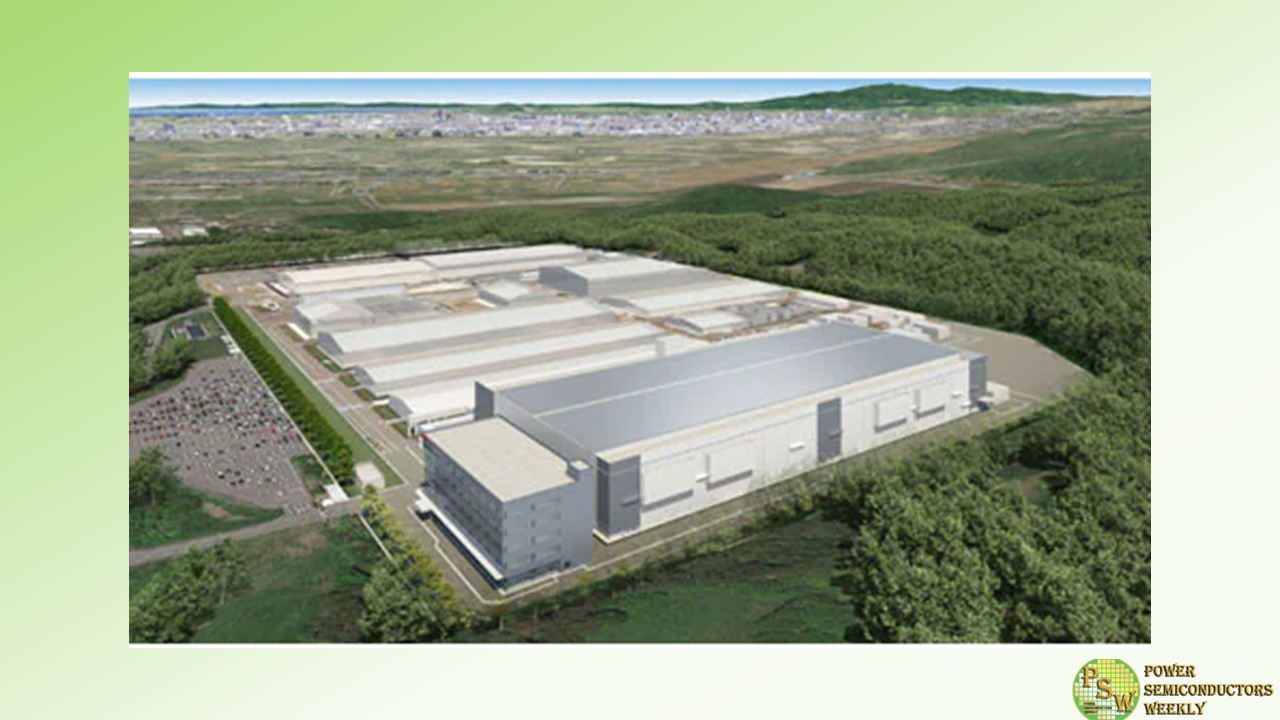
Toshiba Electronic Devices & Storage Corporation (“Toshiba”) announced that it has started construction of a new wafer fabrication factory for power semiconductors at Kaga Toshiba Electronics Corporation, in Ishikawa Prefecture, Japan, its main discrete semiconductor production base. Construction will take place in two phases, with the production start of Phase 1 scheduled for within fiscal 2024. Toshiba will also construct an office building adjacent to the new fab to respond to the increase in personnel.
The new fab will have a quake absorbing structure and enhanced BCP systems, including dual power supply lines, and also aim to use 100% renewable energy. Product quality and production efficiency will be improved by introducing artificial intelligence systems and other measures.
Toshiba started power semiconductor production on a 300-milimeter wafer line in the second half of fiscal 2022. Going forward, Toshiba will expand production capacity of power semiconductors with the new fab and further contribute to carbon neutrality.
Original – Toshiba
-
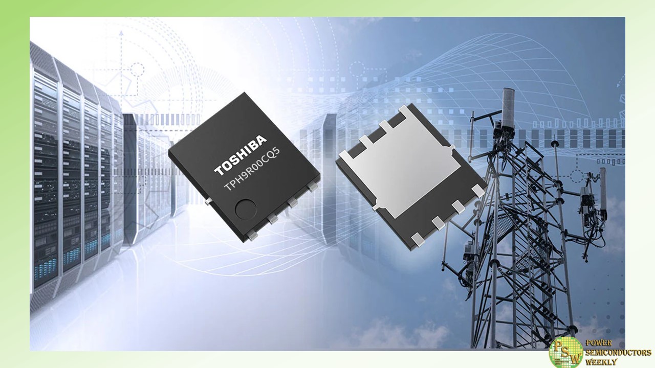
Toshiba Electronic Devices & Storage Corporation has launched a 150V N-channel power MOSFET “TPH9R00CQ5,” which uses the latest generation U-MOSX-H process, for switching power supplies of industrial equipment, such as that used in data centers and communications base stations.
TPH9R00CQ5 features an industry-leading low drain-source On-resistance of 9.0mΩ (max), approximately a 42% reduction from Toshiba’s existing product, “TPH1500CNH1.” Compared with Toshiba’s existing product “TPH9R00CQH,” the reverse recovery charge is reduced by about 74% and the reverse recovery time by about 44%, both key reverse recovery characteristics for synchronous rectification applications. Used in synchronous rectification applications, the new product reduces the power loss of switching power supplies and helps improve efficiency. Furthermore, compared to TPH9R00CQH, the new product reduces spike voltage generated during switching, helping lower the EMI of power supplies.
The product uses the popular, surface-mount-type SOP Advance(N) package.
Toshiba also offers tools that support circuit design for switching power supplies. Alongside the G0 SPICE model, which verifies circuit function in a short time, highly accurate G2 SPICE models, which accurately reproduce transient characteristics, are now available.
Toshiba has also developed “1 kW Non-Isolated Buck-Boost DC-DC Converter for Telecommunications Equipment” and “Three-phase Multi Level Inverter using MOSFET” reference designs that utilize the new product. They are available on Toshiba’s website from today. The new product can also be utilized for the already published “1 kW Full-Bridge DC-DC Converter” reference design.
Toshiba will continue to expand its lineup of power MOSFETs that reduce power loss, increase the efficiency of power supplies, and help to improve equipment efficiency.
Applications:
- Power supplies of industrial equipment, such as that used in data centers and communications base stations.
- Switching power supplies (high efficiency DC-DC converters, etc.)
Features:
- Industry-leading low On-resistance: RDS(ON)=9.0mΩ (max) (VGS=10V)
- Industry-leading low reverse recovery charge: Qrr=34nC (typ.) (-dIDR/dt=100A/μs)
- Industry-leading fast reverse recovery time: trr=40ns (typ.) (-dIDR/dt=100A/μs)
- High channel temperature rating: Tch (max)=175°C
Original – Toshiba
