-
LATEST NEWS / PROJECTS / SiC / WBG
Tianjin Economic-Technological Development Area Inked Investment Agreement with Vitesco Technologies
1 Min ReadTianjin Economic-Technological Development Area (TEDA) inked an investment agreement with Vitesco Technologies for a new project for NEV intelligent manufacturing and automotive electronic products. With the new project, Vitesco aims to strengthen its presence in TEDA by introducing new products such as silicon carbide power modules, 800V motor stators and rotors, EMR3 three-in-one axle drive systems, high-voltage inverters, battery control units, and gearbox controllers.
Vitesco Technologies is a global leader in automotive technology development and manufacturing, dedicated to providing advanced driving technology for sustainable mobility. Vitesco Technologies has been cooperating with TEDA for many years.
The establishment of its R&D center in TEDA in 2019 marks a major step forward in the NEV market, upgrading the Vitesco Tianjin Base into a super factory integrating R&D, testing, and production. Thomas Stierle, member of the Executive Board and head of Electrification Solutions Division of Vitesco Technologies, expressed confidence in China, Tianjin, and TBNA. He stated that Vitesco Technologies will continue to increase its investment in TBNA and deepen cooperation in manufacturing R&D and technological innovation.
-
INDUSTRY PAPERS23 Min Read
Abstract
A SiC double-trench MOSFET embedded with a lower-barrier diode and an L-shaped gate-source in the gate trench, showing improved reverse conduction and an improved switching performance, was proposed and studied with 2-D simulations. Compared with a double-trench MOSFET (DT-MOS) and a DT-MOS with a channel-MOS diode (DTC-MOS), the proposed MOS showed a lower voltage drop (VF) at IS = 100 A/cm2, which can prevent bipolar degradation at the same blocking voltage (BV) and decrease the maximum oxide electric field (Emox).
Additionally, the gate–drain capacitance (Cgd) and gate–drain charge (Qgd) of the proposed MOSFET decreased significantly because the source extended to the bottom of the gate, and the overlap between the gate electrode and drain electrode decreased. Although the proposed MOS had a greater Ron,sp than the DT-MOS and DTC-MOS, it had a lower switching loss and greater advantages for high-frequency applications.
1. Introduction
Nowadays, silicon carbide (SiC) is widely used in many applications because of its high critical electric field and superior thermal conductivity. The SiC MOSFET has a lower on-resistance and a faster switch speed compared with the Si-insulated Gate Bipolar Translator (IGBT). However, the body diode of the SiC MOSFET has a high on-state voltage drop of about 2–3 V because of its wide bandgap.
Additionally, when the body diode operates in bipolar mode, basal plane dislocations (BPDs) and stacking faults (SFs) are generated because of the recombination energy of the electrons and holes, and these faults cover most of the junction area and cause conduction losses to increase. Thus, the SiC MOSFET usually reverse-parallels a freewheeling diode to suppress the body diode; this extra diode not only increases the package size but also increases the parasitic inductance, which limits the switching frequency of the MOSFET.
One possible way of solving this problem is to integrate a unipolar diode into the MOSFET cell—in particular, a Schottky Barrier Diode (SBD)/Junction Barrier Controlled Schottky Diode (JBS). A disadvantage of these integrated unipolar diodes is the increased leakage current in the blocking state for the MOSFET. The use of a built-in channel diode is another option that can improve the reverse-recovery characteristics of the MOSFET, showing better switching characteristics, but the reliability problem caused by thin gate oxide still needs further research.
In recent research, low-barrier diodes (LBDs) have been adopted for their enhanced third-quadrant and switching performance in planar MOSFETs, but the planar structure limits the MOSFET’s usage in high-power applications because of its wide cell pitch and its high specificity of resistance (Ron,sp).
This paper proposes a 1200 V L-shaped split-gate trench SiC MOSFET integrated with a low-barrier diode. This structure can inhibit the reverse conduction of the body diode to avoid the effects of bipolar degradation and to extend the source to the bottom of the gate, forming a split gate to reduce the Crss and to achieve a fast switching speed.
This study was carried out with numerical TCAD, and some essential models were included such as the Fermi–Dirac, incomplete-ionization, Shockley–Reed–Hall and Auger combination, Lombardi (CVT), impact-ionization, and band-narrowing models. A channel mobility of 50 cm2/(Vs) was used. The structure achieved a lower VF, Cgd, and Qgd and lower switching losses compared with a DT-MOS and a DT-MOS with an MOS-channel diode (DTC-MOS), and it also reduced the maximum oxide electric field (Emox).
2. Device Structure and Mechanism
Figure 1 shows the schematic structures of the (a) DT-MOS, (b) DTC-MOS, and (c) proposed MOS. Based on the DTC-MOS, the proposed MOS turns part of the polysilicon gate to the source and extends to the bottom of the gate, forming an “L-shape” split gate. The gate-source connects to the source, so the overlap between the gate and drain decreases, which leads to a decrease in the Cgd. Meanwhile, at the right half-cell, the p-base turns into an n-base, so a low-barrier diode is integrated into this structure to improve its reverse conduction. The P-shield extends to the current spreading layer (CSL), and it decreases the Emox in the blocking state and increases the BV, improving the device’s reliability.
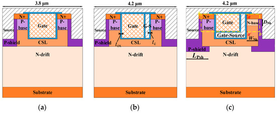
Figure 1. Schematic cross-sectional structures of the (a) DT-MOS, (b) DTC-MOS, and (c) proposed MOSFET.
This device is based on a 4H-SiC, with the doping concentration and thickness of the N-drift set at 8 × 1015 cm−3 and 9 μm, respectively. The P-base region in all the devices had a doping concentration of 2 × 1017 cm−3 and a thickness of 0.5 μm. The N-base had a doping concentration of 3 × 1016 cm−3 and a thickness of 0.3 μm. The P-shield had a doping concentration of 2 × 1018 cm−3 and a thickness of 0.3 μm. The CSL had a doping concentration of 8 × 1016 cm−3 and a depth of 1.7 μm. The depth of the source trench and gate trench was 1.4 μm for both devices. The thickness of the gate oxide was 50 nm for both the N-base and P-base to improve the device reliability in the DT-MOS and proposed MOS. Considering the sufficient volume of the gate and the electric field, the distance of the oxide between the gate and gate-source and the thickness of the gate-source was 0.1 μm for the DTC-MOS and the proposed MOS. The cell pitch was 3.8 μm for the DT-MOS, and that of the other two devices was 4.2 μm. The main structure parameters of the DT-MOS, DTC-MOS, and proposed MOS are shown in Table 1.
Table 1. Structural parameters of the three devices.
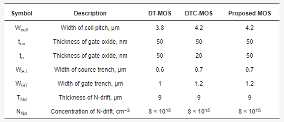
Figure 2a shows the three-dimensional conduction band energy (EC) distribution of the 4H-SiC in the proposed MOS structure at zero bias. The EC decreased from the P-shield to the N-base at the right half-cell. The high doping of the P-shield and the low doping of the N-base led to a rapid depletion of the N-base region at zero bias, preventing the formation of a conducting channel. Therefore, there was no impact on the BV at low doping concentrations.
At zero bias, the EC of the N-base was lower than the P-base, allowing electrons to overcome the potential barrier at a low Vds. Figure 2b shows the EC distribution along the a–a’ line (shown in Figure 1) at different Vds. As Vds decreased, the EC increased in both the N-base and CSL. However, the EC of the CSL increased faster than the N-base region. At Vds = −1 V, the potential barrier became very low, allowing electrons to overcome the potential barrier, turning on the low barrier diode.
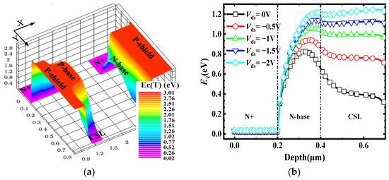
Figure 2. (a) Three-dimensional EC distribution of the proposed MOSFET at zero bias (b–b’—the yellow dashed line in Figure 1). (b) EC distribution of the SiO2/SiC interface (a–a’—the red dashed line in Figure 1) at different Vds.
The potential barrier model for LBD in a planar MOSFET is given by:

where ϕSi_SiCand χSi_SiCare the work function and electron affinity difference between the Si and SiC. ɛOX and ɛSiC are the permittivity of the SiO2 and SiC. NNb is the doping concentration of the N-base. The WNb is the width of the N-base. The structure of the low barrier diode in a planar structure and trench structure is the same, being formed by the N+ polysilicon, oxide, the low doping concentration N region, and the high doping concentration P region. Although the formula was obtained for planar structures, it is also applicable to trench structures.
The tc is the thickness of the oxide between the gate-source and the N-base, which is fixed at 50 nm in the proposed MOS, as it has a great influence on device reliability. The tc of the DTC-MOS was 20 nm, to easily turn on the built-in diode. From equation (1), NNb and WNb had an impact on the potential barrier of the LBD. Additionally, the thickness of the N-base (TNb) and the length of the P-shield (LPsh) also influenced the resistance of the LBD, which in turn affects the VF. Therefore, these parameters were optimized.
3. Simulation Results and Analysis
Figure 3a illustrates the impact of WNb and DNb on the BV and VF. The solid circles represent BV values and the dashed circles represent VF values. The WNb varied from 0.1 μm to 0.6 μm in steps of 0.1 μm. As WNb increased, the reverse current path expanded, which led to a decrease in VF. However, the breakdown turned into a punch-through breakdown, which made the device unable to withstand high voltages.
With increasing DNb, the length of the potential barrier increased, leading to an increase in VF. In this case, a longer WNb was required to trigger a punch-through breakdown. It is worth noting that when DNb exceeded 0.3 μm, the leakage current of the proposed MOS became comparable to the DT-MOS, which will be further discussed later. To tradeoff the BV, VF, and leakage current, the optimal values of WNb = 0.3 μm and DNb = 0.3 μm were selected.
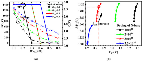
Figure 3. (a) Influence of DNb and WNb on BV and VF; (b) BV, VF at different LPsh and NNb.
Figure 3b shows the tradeoff between the BV and VF for the proposed MOS, considering different values of LPsh and NNb. As the LPsh increased from 1 μm to 1.5 μm in steps of 0.1 μm, the depletion region extended, leading to a decrease in Emox and an increase in BV. However, the current path became narrow, leading to an increase in Ron,sp and VF because of the change in the JFET resistance. With increasing NNb, the potential barrier of the low barrier diode reduced, leading to a decrease in VF.
However, with high doping of NNb, the BV dropped below 1400 V, as shown for NNb = 3.5 × 1016 cm−3. At low NN values, the breakdown point occurred at the P-shield/N-drift junction, so the BV did not change with different NNb values. The change in NNb had no influence on Ron,sp. However, with increasing LPsh, the Ron,sp increased from 1.84 mΩ × cm−2 to 4.58 mΩ × cm−2. In order to tradeoff BV, VF, and Ron,sp, LPsh = 1.3 μm and NNb = 3 × 1016 cm−3 were selected, represented by the red circle in Figure 3b.
The main parameters of the gate trench are shown in Figure 4a. The thickness of the gate trench was fixed at 1.4 μm. Figure 4b shows the influence of the distance between the gate and the gate-source (Dox) on the Cgd and oxide electric field (Eox). The voltage between the gate and the gate-source was set to 15 V. When Dox was 0.1 μm for both the bottom and side wall of the gate, the Eox was 1.5 MV/cm, which corresponds to the simulation results.
The thickness of the gate-source (TGS) was fixed at 0.1 μm, and the thickness of gate poly (TG) changed as Dox increased or decreased. With increasing Dox, the BV and VF had no influence, so they are not included in Figure 4b. The Dox has little influence on Cgd. Therefore, when Dox was greater than 0.1 μm, Eox was already less than 3 MV/cm. In order to facilitate subsequent simulations and ensure a sufficient volume of gate poly for adjusting the gate resistance, Dox = 0.1 μm was selected.
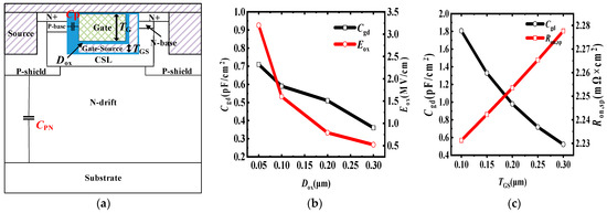
Figure 4. (a) Parasitic capacitance for the Cgd of the proposed MOS. (b) Influence of device characteristics on the distance between the gate and gate-source (c) Influence of Cgd and Ron,sp on the thickness of the gate-source.
The influence of the device characteristics on TGS is shown in Figure 4c; the Dox was fixed at 0.1 μm. With increasing TGS, there was no influence on BV and VF, which is not shown in the figure. Ron,sp increased from 2.23 mΩ∙cm2 to 2.28 mΩ∙cm2, because the CSL, oxide, and gate poly formed an MIS structure, which increased the electron concentration of the CSL during conduction; this effect weakened as TG decreased.
With increasing TGS, Cgd decreases; this is because the gate-source extends to the bottom of the gate poly, resulting in a significant decrease in the overlap between the gate electrode and drain electrode. In this case, the Cgd can be expressed as:

As shown in Figure 4a, Cp is the oxide capacitance between the P-base and gate electrode, which is related to the thickness of the oxide and the overlap between the gate poly and the P-base. CPN is the junction capacitance, which is completely independent of the gate parameters, and the CPN decreases as Vds increases. When increasing TGS or Dox, the TG decreases, resulting in a decreased overlap between the gate poly and the P-base, thus causing a decrease in Cp.
Meanwhile, the TG has no influence on CPN, so the Cgd will decrease. However, it is worth noting that the Cgd is already sufficiently small, and further decreasing Cp cannot significantly change the Cgd. To ensure a suitable gate resistance for device, a sufficient volume of gate poly must be considered, which cannot be reflected in a simulation. Therefore, TGS = 0.1 μm was selected for further simulations.
According to Figure 4b,c, the internal parameters of the gate trench have little influence on the performance of the device when the resistance of the gate poly is not considered; this shows that the proposed MOS has a wide process window for forming the L-shape gate-source.
Figure 5a shows the leakage current and blocking voltage for the three devices. The DT-MOS and proposed MOS blocking voltage exceeded 1400 V. However, the BV of the DTC-MOS was only 1340 V. This indicates that a wide cell pitch results in a decrease in the BV, while the extended P+ shield helps to improve the BV. For the proposed MOS, the leakage current increased faster at DNb = 0.2 μm.
However, when DNb = 0.3 μm, the BV was the same as DNb = 0.2 μm, the leakage current decreased to the level of the DT-MOS. This is because the leakage current is related to the parameters of the N-base before breakdown and the blocking voltage is related to the P-shield/N-drift junction, where the electric field is highest in the SiC region and avalanche breakdown occurs.
The electric field distribution of the three devices at 1200 V is shown in Figure 5b. The Emox was located at the bottom of the oxide for all the devices. Compared with the DT-MOS and DTC-MOS, the proposed MOS had an extended P-shield, which was able to expand the depletion layer and provide better protection effects to the oxide. As a result, the Emox was only 2.52 MV/cm, while the Emox of the other devices was higher than 4 MV/cm.
With a high Emox, a Fowler–Nordheim tunneling current may be generated; this carries electrons through the oxide layer, breaking the Si-O bond over time and generating defects, leading to a full breakdown of the SiO2 layer, which has a great influence on device reliability.
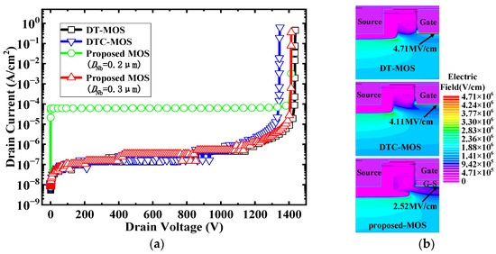
Figure 5. (a) BV characteristics (b) electric field distributions with a drain bias at 1200 V of the DT-MOSF, DTC-MOS, and proposed MOS.
The I–V characteristic is shown in Figure 6a. In forward conduction, the Ron,sp of the DT-MOS and DTC-MOS was smaller than for the proposed MOS; this is because the DT-MOS has two channel paths for conduction, and because both DT-MOS and DTC-MOS do not extend the P-shield, which increases JFET resistance. With a low barrier diode, the VF of the proposed MOS decreased significantly. The VF was 2.85 V, 2.63 V, and 0.85 V at 100 A/cm2 for the DT-MOS, DTC-MOS, and proposed MOS, respectively.
The current vector of the forward and reverse conduction is also shown in Figure 6a. It can be seen that there was only one current path for both conduction conditions. The current flows from the N+ region through the N-base to the drift region in reverse conduction, while the current flows from the drift region through the P-base to the N+ region in forward conduction. Figure 6b shows the hole concentration at Is = 100 A/cm2 of all the devices. In reverse conduction, the drift region of the DT-MOS obtained a high concentration of holes, which causes bipolar degradation.
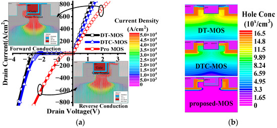
Figure 6. (a) I–V characteristics of the three devices; (b) hole concentration distributions at Is = 100 A/cm2.
The short-circuit (SC) test results for the DT-MOS, DTC-MOS, and proposed MOS are shown in Figure 7. The SC test circuit used in the simulation is shown in Figure 7b. The bus voltage was 800 V. The stray inductance and resistance was 1 nH and 1 mΩ, respectively. The gate resistance was 10 Ω. A single pulse of 0 V/15 V gate bias was applied to the gate contact until the device failed due to thermal runaway caused by excessive temperatures.
The time from device turn-on to failure was 1.6 μs, 1.9 μs, and 2.8 μs for the DT-MOS, DTC-MOS, and proposed MOS, respectively. For the DT-MOS, the highest saturation current caused a faster temperature rise, leading to earlier device failure. Due to the single current channel and depletion layer extension of the P-shield region, the proposed MOS exhibited the lowest saturation current. As a result, the proposed MOS achieved the longest time until failure.
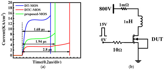
Figure 7. (a) Short circuit characteristics of the three devices; (b) short-circuit test circuit.
In the proposed MOS, the gate-source extended to the bottom of the gate, leading to a decrease in the overlap between the gate and the drain. As a result, the proposed MOS had the lowest Cgd compared to the DT-MOS and DTC-MOS, as shown in Figure 8a. While switching transients, the time constant is determined by the junction capacitance and gate resistors, which impact the switching speed of the devices. With a smaller capacitance, the devices switch at a faster speed.
The Cgd was 141.68 pF/cm2, 136 pF/cm2, and 1.81 pF/cm2 for the DT-MOS, DTC-MOS, and proposed MOS, respectively. Figure 8b shows the gate charge for the three devices; the Qgd of the DT-MOS was 569 nC/cm2 and the Qg (Vgs = 15 V) was 1467 nC/cm2. The Qgd of the DTC-MOS was 406 nC/cm2 and the Qg was 1136 nC/cm2. However, the Qgd of the LST-MOSFET was 6.7 nC/cm2 and the Qg was 333 nC/cm2; this result is consistent with the results for the Cgd, indicating that the proposed MOS can significantly reduce switching losses.
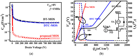
Figure 8. (a) C–V characteristics; (b) Gate Charge of three devices.
The switching waveforms and test circuit of the three devices are shown in Figure 9. Figure 9d shows the resistance switch circuit used in the simulation, with a load current of 10 A (100 A/cm2) at a normal current density. As can be seen in Figure 9a, the proposed MOS exhibited a lower Qgd compared to the other devices. The miller plateau almost disappeared, leading to a faster transition of Vgs, which is consistent with the Cgd results. This characteristic resulted in a significantly faster switching speed for the proposed MOS compared to the other devices, thereby reducing switching losses.
From Figure 9b, the turn-on loss (Eon) and turn-off loss (Eoff) of the DT-MOS was 0.28 mJ/cm2 and 0.47 mJ/cm2 and for the DTC-MOS was 0.26 mJ/cm2 and 0.48 mJ/cm2. However, for the proposed MOS, the Eon and Eoff decreased to 0.09 mJ/cm2 and 0.29 mJ/cm2. The switching losses (ESW) consisted of the Eon and Eoff; the ESW of the proposed MOS was 49.3% and 48.6% lower than that of the DT-MOS and DTC-MOS, respectively.
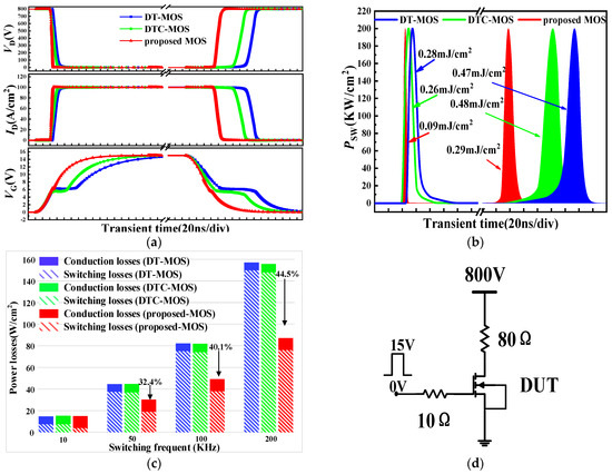
Figure 9. The switching waveforms of the DT-MOS, DTC-MOS, and Proposed MOS, respectively; (a) Turn-on and turn-off waveforms; (b) Turn-on loss and turn-off loss waveforms; (c) total power losses as a function of switching frequency f; (d) resistance switching circuit for simulations.
The total power losses (Pt) consist of conduction power losses and switching losses. When the device is operating under a square wave with a period T and a duty cycle D, the Pt can be expressed as (3):

When the device operated at 100 A/cm2, the Vds was 0.132 V, 0.156 V, and 0.223 V for the DT-MOS, DTC-MOS, and proposed MOS, which is consistent with the Ron,sp. The switching frequency, f, is related to the period, T, by the formula

Although the Ron,sp of the proposed MOS was greater than that of the DT-MOS and DTC-MOS, the switching losses were the main contributor to power loss at high frequencies. Working at high frequencies can effectively reduce the total power losses of the device; it is worth it to increase the on-resistance slightly to achieve smaller switching losses at high frequencies.
Figure 9c shows the total power loss as a function of f for the three devices, when a D of 50% was assumed. When the switching frequency was 50 KHz, the proposed MOS achieved the lowest power loss compared to the other devices due to its lower switching loss. At a switching frequency of 200 KHz, the Pt of the proposed MOS was 44.5% lower than the DT-MOS. With increasing f, the deference in Pt between the DT-MOS and the proposed MOS gradually increased.
The switching condition at a high current density (500 A/cm2) is shown in Figure 10. As the current density increased, both conduction losses and switching losses increased significantly. The ESW of the three devices is shown in Figure 10a. The proposed MOS value was 0.96 mJ/cm2, which was 42.9% and 36.4% lower than the DT-MOS and DTC-MOS.
However, the conduction losses of the proposed MOS increased faster than the other devices at 500 A/cm2. As a result, the Pt of the proposed MOS was the highest before f = 200 KHz, as shown in Figure 10b. At a f of 250 KHz, the Pt of the proposed MOS was only 7.6% lower than that of the DT-MOS. Comparing the work conditions between a normal current density and a high current density, it is more favorable for the proposed MOS to work at a normal current density.
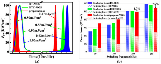
Figure 10. Device works at 500 A/cm2; (a) Turn-on loss and turn-off loss waveforms; (b) total power losses as a function of switching frequency f.
However, high switching speeds and frequencies may present a greater switching oscillation challenge. By adding RC snubbers, reducing the switching speed, or using active gate control techniques, the switching oscillation will be suppressed. However, the mentioned methods for suppressing switching oscillation will lead to an undesirable increase in switching time and switching losses.
There is a tradeoff between power losses and switching oscillation. An electronic structure that has transient part-time symmetry triggered by the switching-on and off of electronic devices can release oscillation energy, while still maintaining the very low loss state. This may be a good choice for suppressing switching oscillation in the future. The comprehensive performance of the three devices is shown in Table 2.
Table 2. Comparison of the three devices’ characteristics.
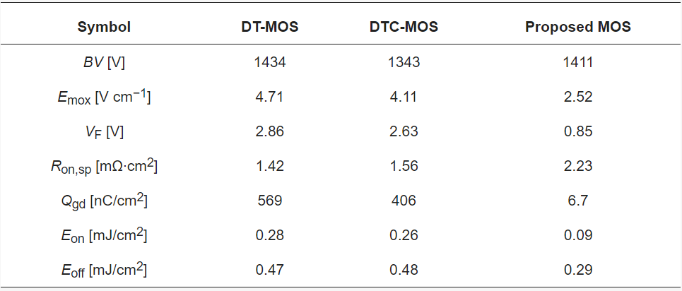
Figure 11 shows a possible process for the proposed MOS. The process starts with the formation of the P-shield region after epitaxy, as shown in Figure 11a. Then, the P-base and N-source are formed by ion implantation followed by high-temperature annealing, as shown in Figure 11b. After this, the gate trench is etched, the gate oxide is formed by chemical vapor deposition (CVD), and the polysilicon is deposited and etched to form the gate-source, which is shown in Figure 11c.
Then, the oxide is deposited and the N+ polysilicon is deposited and etched to form the gate electrode, which is shown in Figure 11d. Figure 11e shows the etching of the source trench and tilted implantation to form the P+ region along the sidewall of the source trench. Finally, Figure 11f shows the deposition of a passivation layer, the etching of the contact window, and the formation of the ohmic contact.
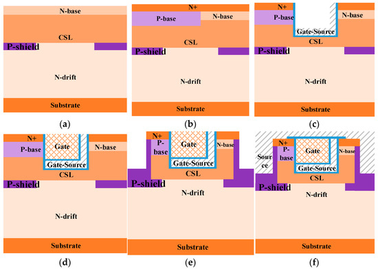
Figure 11. Key fabrication process flows for the proposed MOSFET: (a) Form P-shield layer. (b) Form P-base layer and N-source layer. (c) Etch to form gate trench and form oxide by CVD to form the gate oxide; deposit and etch polysilicon to form gate-source. (d) Deposit oxide and polysilicon to form gate. (e) Etch to form source trench and ion implantation to form the P+. (f) Form source electrode.
4. Conclusions
In this paper, a SiC novel MOSFET is proposed and studied by TCAD simulations. The proposed MOS integrates a low barrier diode and has a gate-source structure located under the bottom of gate. The simulation results demonstrate that the proposed MOSFET has a smaller VF compared to the DT-MOS and DTC-MOS because of the low barrier diode, which suppresses the conduction of the body diode.
This allows the proposed MOS to operate under unipolar operations with reverse conduction, preventing the effects of bipolar degradation. The influence of the main parameters of LBD on device performance has been studied, and the optimal value has been determined. Additionally, the length of the P-shield has been studied to achieve a low Emox and high blocking voltage. The parameters of the gate trench have also been studied, which show a high process tolerance for forming an L-shape without affecting the static performance.
In addition to the static performance, the Cgd and Qgd of the three devices were compared. Due to a reduction in the overlap between the gate electrode and drain electrode, the proposed MOS achieved the lowest Cgd and Qgd. As a result, the proposed MOSFET is able to achieve better switching speeds and lower switching losses.
The proposed MOS achieved the lowest total power losses under 50 KHz and higher switching frequencies with a normal current density. This indicates that the proposed MOSFET has more advantages in high frequency switching applications.
Authors
Yangjie Ou, Zhong Lan, Xiarong Hu, Dong Liu.
Original – MDPI
-
LATEST NEWS / PRODUCT & TECHNOLOGY / SiC / WBG4 Min Read
Vitesco Technologies is preparing the series application of its High Voltage Box. The modular system makes charging, converting and distributing electricity in electric vehicles cheaper by integrating several functions in one unit, depending on the design.
This includes the vehicle On-Board Charger for AC charging on the grid with up to 22 kW of charging power, a DC current converter providing the current for the 12 V vehicle net, and power electronics which distribute high voltage power in the vehicle and facilitate fast DC-charging with up to 800 V.
Owed to the high level of mechatronic integration, the High Voltage Box has smaller space requirements to the vehicle while increasing the total system reliability in comparison to individual devices. State-of-the art silicon carbide (SiC) semiconductors boost charging efficiency to over 95 percent which lowers the vehicle owner’s electricity bill. This efficiency level is particularly beneficial for car owners because electric vehicles are frequently charged on the grid.
Due to the high AC charging rate of up to 22 kW the High Voltage Box charges the car with 200 km of range in under two hours. DC high-power charging with up to 800 V achieves the same range in 12 minutes. The sophisticated power electronics ensure that this system offers electrical safety as well as efficiency.
On a day-to-day level, charging, energy conversion and power distribution are just as relevant for a driver’s satisfaction with a vehicle as driving itself is. With our High Voltage Box, we integrate these core tasks of energy management into one efficient and compact unit. This integration makes electrification on a large scale and at low cost easier.
Thomas Stierle, Member of the Executive Board and head of the Electrification Solutions division of Vitesco Technologies
Today, the so-called On-Board Charger (OBC) for charging with alternating current (AC) on the grid is a separate device in the vehicle. This OBC inverts grid power to direct current (DC) that can be fed to the high voltage battery. Another separate device is the DC/DC converter which provides direct current from the high voltage battery to the 12 V power net – or it boosts 12 V to high voltage DC. A power electronics unit distributes high voltage current within the vehicle (hence: Power Distribution Unit, PDU). In addition, these electronics can be designed to allow DC charging with up to 800 V at high power charging points. All those components need to be connected, they require a housing, installation space, and cooling.
The modular and scalable High Voltage Box makes it easier to cover two or more of these functions with a single device. SiC technology is used to minimize the conversion losses of the unit:
A high level of efficiency brings the car owner’s electricity bill down and contributes to sustainability.
Christian Preis, Head of Base Development Energy Transformation at Vitesco Technologies
Within the modular design Vitesco Technologies covers all relevant European and worldwide grid topologies. The High Voltage Box was developed to support modular vehicle adaptation for the global market. At the same time, Vitesco Technologies is driving new functions ahead. The High Voltage Box for one of the two series applications will already function bidirectionally so that it can supply alternating current with 230 V from the DC battery current when this is required.
This puts vehicle owners in the comfortable position to make versatile use of their large battery. For instance, if they wish to use power tools far away from the grid, or if they want to feed electricity to the grid which they have charged earlier from their own photovoltaic system. “In the future, this option to stabilize the grid will continue to gain importance “, Preis adds. The company’s experts are advancing the necessary standard for this in key committees and are thus part of the decision-making process about development trends.
In the future the High Voltage Box with bidirectional function can also make it possible to power a whole house from the High Voltage Battery during a blackout. This is an option because batteries in vehicles have a much bigger capacity than most of the batteries typically installed in private homes.
Original – Vitesco Technologies
-
Cambridge GaN Devices (CGD) is addressing higher power industrial applications with its ICeGaN™ technology which has already proved itself rugged, reliable and easy-to-use in high volume consumer devices. At the APEC 2024, IEEE Applied Power Electronics Conference and Exposition, the company is introducing new reference designs and showing demos which address the broad and diverse industrial market.
Andrea Bricconi | Chief Commercial Officer, CGD
“We are acutely aware of the increasing power requirements of industrial applications, and the need for high efficiency. For example, as the use of Artificial Intelligence (AI) proliferates, the power demanded by the exponential growth in power demanded by datacentres is growing almost exponentially. Other applications, such as solar inverters, amplifiers, transport and smart mobility, process control and manufacturing are also interested in GaN and the feedback we have received is that they love the simplicity of our ‘Drive it Like a MOSFET’ approach.”
At APEC, visitors to the booth are able to see the progress that CGD is making to support both emerging and existing markets for GaN technology..
With a high power density of 23 W/in3, GGD’s 350 W PFC/LLC reference design has an average efficiency of 93%, and a no-load power consumption of 150 mW. The CrM Totem Pole PFC + Half-Bridge LLC PSU has been realised using CGD’s 650 V, 55 mΩ, H2 series ICeGaN technology, and delivers 20 V / 17.5 A output.
The result of a partnership deal struck last year with Neways Electronics, a 3 kW photo-voltaic inverter is used to boost the DC solar voltage to a stable DC link voltage. With a maximum efficiency of 99.22% due to zero-current switching, it is a perfect example of how CGD’s GaN HEMT structure is simple for engineers to use, since it employs a standard silicon controller from Analog Devices Inc.
ICeGaN has been employed by AGD Productions in its compact AGD DUET amplifier which is rated at 300W 4Ω. This is the first time the company has used a 100% GaN power transistor design for both the power stage and the amplifier.
Finally, the GaNext project, a consortium of 13 partners from three nations has delivered compact 1 kW intelligent power modules featuring integrated drive, voltage control and protection circuits using CGD’s ICeGaN.
Original – Cambridge GaN Devices
-
GaN / LATEST NEWS / PRODUCT & TECHNOLOGY / WBG2 Min Read
Power Integrations announced the InnoMux™-2 family of single-stage, independently regulated multi-output offline power-supply ICs. InnoMux-2 ICs consolidate AC-DC and downstream DC-DC conversion stages into a single chip, providing up to three independently regulated outputs for use in white goods, industrial systems, displays and other applications requiring multiple voltages.
Elimination of separate DC-DC stages slashes component count, reduces PCB footprint and increases efficiency by as much as 10 percentage points compared to traditional two-stage architectures. Efficiency is aided by the ICs’ 750 V PowiGaN™ gallium-nitride transistors, zero-voltage switching (without an active clamp) and synchronous rectification.
Roland Saint-Pierre, vice president of product development at Power Integrations said: “Most modern electronic systems rely on multiple internal voltages to operate various functions such as computing, communication and actuation function – typically heat, light, sound or motion of some kind. But losses in each conversion stage are compounded, degrading system performance and generating heat.
The InnoMux-2 IC overcomes this challenge by providing up to three independently regulated voltage outputs or two voltage output and a constant current output from a single stage, achieving a compact and efficient power sub-system with low component count.”
InnoMux-2 ICs deliver up to 90 watts of output power with accurate regulation of better than ±3 percent across the full input line, load, temperature and differential current step conditions. Total power system efficiency (AC to regulated low-voltage DC segment) is above 90 percent; the advanced InnoMux-2 controller also manages light-load power delivery, avoiding the need for pre-load resistors and reducing no-load consumption to less than 30 mW. This conserves power for necessary functionality in applications subject to the 300 mW allowance for standby usage under the European energy-using product (EuP) regulations.
InnoMux-2 devices leverage Power Integrations’ thermally efficient InSOP™24 and InSOP™28 packages with PCB cooling, so no heatsink is required. Device options include dual- and three-output constant voltage (CV); optionally, one output may be dedicated to constant current (CC) drive, suitable for powering LEDs in displays or for high-speed charging of an internal battery. Typical applications include TVs, monitors, appliances, networking, home and building automation, LED emergency lighting and industrial power supplies.
Original – Power Integrations