-

onsemi has unveiled plans to acquire Qorvo’s Silicon Carbide (SiC) JFET business, a strategic move that enhances its portfolio in high- and mid-voltage power semiconductors. The $115 million deal includes Qorvo’s United Silicon Carbide subsidiary and is expected to close in Q1 2025. This acquisition is projected to expand onsemi’s market opportunity by $1.3 billion by 2030, focusing on AI, data centers, EVs, and industrial markets. By leveraging its vertically integrated SiC supply chain, onsemi aims to boost efficiency, profitability, and innovation across key technology areas.
SiC JFET technology offers superior power efficiency, reduced costs, and versatility in advanced applications, including EV battery systems, AI-driven data centers, and renewable energy solutions. It promises to disrupt traditional silicon-based and GaN technologies, with its superior switching speed, lower on-resistance, and smaller die size. This acquisition positions onsemi to capitalize on the growing demand for sustainable, high-performance power solutions in a wide range of industries.
Moreover, SiC JFETs are designed to enable transformative advancements in industrial applications such as power supplies, solar power converters, and energy storage systems. These innovations align with market trends emphasizing higher efficiency and reliability. The technology also offers critical advantages in EV battery safety, ensuring quicker response and long-term dependability through solid-state switches that surpass conventional electromechanical solutions.
By integrating Qorvo’s business, onsemi also strengthens its presence in the competitive AI and data center markets. The shift to higher voltages and power capacities in these areas provides a unique opportunity for SiC JFETs to reduce costs and improve performance, establishing onsemi as a leader in next-generation semiconductor solutions.
Original – onsemi
-

ROHM and TSMC have entered a strategic partnership on development and volume production of gallium nitride (GaN) power devices for electric vehicle applications.
The partnership will integrate ROHM’s device development technology with TSMC’s industry-leading GaN-on-silicon process technology to meet the growing demand for superior high-voltage and high-frequency properties over silicon for power devices.
GaN power devices are currently used in consumer and industrial applications such as AC adapters and server power supplies. TSMC, a leader in sustainability and green manufacturing, supports GaN technology for its potential environmental benefits in automotive applications, such as on-board chargers and inverters for electric vehicles (EVs).
The partnership builds on ROHM and TSMC’s history of collaboration in GaN power devices. In 2023, ROHM adopted TSMC’s 650V GaN high-electron mobility transistors (HEMT), whose process is increasingly being used in consumer and industrial devices as part of ROHM’s EcoGaN™ series, including the 45W AC adapter (fast charger) “C4 Duo” produced by Innergie, a brand of Delta Electronics, Inc.
“GaN devices, capable of high-frequency operation, are highly anticipated for their contribution to miniaturization and energy savings, which can help achieve a decarbonized society. Reliable partners are crucial for implementing these innovations in society, and we are pleased to collaborate with TSMC, which possesses world-leading advanced manufacturing technology” said Katsumi Azuma, Member of the Board and Senior Managing Executive Officer at ROHM. “In addition to this partnership, by providing user-friendly GaN solutions that include control ICs to maximize GaN performance, we aim to promote the adoption of GaN in the automotive industry.”
“As we move forward with the next generations of our GaN process technology, TSMC and ROHM are extending our partnership to the development and production of GaN power devices for automotive applications,” said Chien-Hsin Lee, Senior Director of Specialty Technology Business Development at TSMC. “By combining TSMC’s expertise in semiconductor manufacturing with ROHM’s proficiency in power device design, we strive to push the boundaries of GaN technology and its implementation for EVs.”
Original – ROHM
-

VisIC Technologies announced a new partnership aimed at advancing high-efficiency GaN inverter technology for the EV market. This collaboration will provide automotive OEMs with power semiconductors that exceed silicon carbide (SiC) performance, while offering lower costs at device and system level.
In a recent test conducted at AVL’s state-of-the-art facilities in Germany, an inverter based on VisIC’s GaN-on-Silicon D³GaN components proved an outstanding performance. Mounted on AVL’s e-motor test bench and controlled by AVLs SOP eDrive controls algorithm, the system achieved a benchmark efficiency level of 99.67% at 10kHz, stunningly climbing to over 99.8% efficiency at 5kHz — which outperforms comparable SiC inverters by up to 0.5% and is cutting energy losses by more than 60%.
This breakthrough positions the AVL and VisIC partnership as a compelling option for automakers striving to balance high efficiency with affordability in EV design. It is worth noting that VisIC’s GaN-on-Silicon power devices require significantly less energy and therefore CO2 during the chip production process compared to SiC. They can be produced in widespread 200mm and 300mm silicon foundries, which makes scaling production a straightforward process.
“With AVL, we’re making cutting-edge GaN inverter technology accessible for even more electric vehicles, establishing a new benchmark for efficiency and cost-effectiveness in the industry,” said Gregory Bunin, CTO of VisIC Technologies. “Our partnership reflects a shared commitment to driving EV innovation that’s both impactful and accessible, bringing GaN’s unparalleled performance to a broader market.”
“Working with VisICs new GaN power module for high-power systems enables us to offer our customers cutting-edge solutions that are optimally aligned with the requirements of next-generation drive systems. These include, among other things, high power density combined with reduced overall system costs,” added Dr. Thomas Frey, Head of Segment E-Mobility & E-Drive System at AVL Software and Functions GmbH. “Together, we can significantly advance e-mobility and help reduce the carbon footprint.”
Looking ahead, AVL and VisIC plan to expand their GaN-on-Si platform to include 800V GaN power modules, ensuring that their technology remains scalable and adaptable to the needs of the growing BEV market. This collaboration places AVL and VisIC Technologies at the forefront of GaN inverter technology, establishing new standards for energy efficiency and performance across the EV industry.
Original – VisIC Technologies
-

ROHM has announced the adoption of its EcoSiC™ products, including SiC MOSFETs and SiC Schottky barrier diodes (SBDs) in the HFA/HCA series of 3.5kW output AC-DC power supply units for 3-phase applications from COSEL, a leading power supply manufacturer in Japan. Incorporating ROHM SiC MOSFETs and SiC SBDs into the forced air-cooled HFA series and conduction-cooled HCA series achieves up to 94% efficiency. The HCA series has been mass produced since 2023, while the HFA series began mass production in 2024.
Many industrial applications that handle high power in the industrial sector, including MRI machines and CO2 lasers, require 3-phase power supplies that differ from the single-phase power supplies used in households. COSEL’s AC-DC power supply units – equipped with ROHM’s EcoSiC™ technology that excels in high-temperature, high-frequency, high-voltage environments – are compatible with 3-phase power supplies from 200VAC to 480VAC, contributing to improved power supply efficiency across a wide range of industrial equipment worldwide.
Jun Uchida, General Manager, New Product Development Dept. 2, COSEL Co., Ltd.
“The HFA/HCA series achieve high efficiency despite delivering a high-power output of 3.5kW by incorporating ROHM’s low-loss SiC power devices. Operating at high input voltages typically poses a challenge in reducing losses in high-voltage power devices, but using SiC power devices translates to significantly lower losses compared to conventional solutions, resulting in power supplies that maintains high efficiency and power density even under demanding high-power conditions.”
Akihiro Hikasa, Group General Manager, Power Devices Business Unit, SiC Business Section, ROHM Co., Ltd.
“We are delighted to support COSEL, an industry leader in power supply systems, by providing SiC power devices. A leading company in SiC power devices, ROHM also provides comprehensive power solutions that combine peripheral components. In addition, by addressing customer issues, we also improve device performance by incorporating the insights gained into our products. Going forward, we will continue to collaborate with COSEL to contribute to a sustainable society by enhancing the efficiency of industrial equipment that handle large amounts of power.”
The HFA/HCA series are 3.5kW power supplies featuring a wide input range (200VAC to 480VAC) that meets global power supply requirements. This allows them to be used anywhere in the world without the need to modify the power supply for each region, contributing to the standardization of application designs. Both forced air-cooled (HFA series) and conduction-cooled (HCA series) models – selectable based on operating environment – are available in 48V and 65V output voltage variants that can be used as power sources for a variety of high-power applications such as laser generation and MRI.
Original – ROHM
-

GlobalFoundries has received an additional $9.5 million in federal funding from the U.S. government to advance the manufacturing of GF’s essential gallium nitride (GaN) on silicon semiconductors at its facility in Essex Junction, Vermont.
The funding moves GF closer to large-scale production of GaN chips. With the ability to handle high voltages and temperatures, GaN chip technology is essential for enabling higher performance and greater energy efficiency across a range of RF and high-power control applications including automobiles, datacenter, IoT, aerospace and defense.
With the award, GF will continue to add new tools, equipment and prototyping capabilities to its market-leading GaN IP portfolio and reliability testing as the company moves closer to full-scale manufacturing of its 200mm GaN chips in Vermont. GF is committed to creating a fast and efficient path for customers to realize new innovative designs and products that leverage the unique efficiency and power management benefits of GaN chip technology.
“GF is proud of its leadership in GaN chip technology, which is positioned to make game-changing advances across multiple end-markets and enable new generations of devices with more energy-efficient RF performance and faster-charging, longer-lasting batteries,” said Nicholas Sergeant, vice president of IoT and aerospace and defense at GF. “We appreciate the U.S. government’s partnership and ongoing support of our GaN program. Realizing full-scale GaN chip manufacturing will be a catalyst for innovation, for both our commercial and government partners, and will add resilience and strengthen the semiconductor supply chain.”
The new funding, awarded by the U.S. Department of Defense’s Trusted Access Program Office (TAPO), represents the latest federal investment to support GF’s GaN program in Vermont.
“This strategic investment in critical technologies strengthens our domestic ecosystem and national security, and ensures these assets are readily available and secure for DoD utilization. In concert with key partners, this approach fortifies defense systems, empowering resilience and responsiveness,” said Dr. Nicholas Martin, Director at Defense Microelectronics Activity.
In total, including the new award, GF has received more than $80 million since 2020 from the U.S. government to support research, development and advancements to pave the way to full-scale GaN chip manufacturing.
Vermont is a U.S.-accredited Trusted Foundry and the global hub of GF’s GaN program, with longstanding leadership in 200mm semiconductor manufacturing. In July 2024, GF acquired Tagore Technology’s Gallium Nitride Power portfolio and created the GF Kolkata Power Center in Kolkata, India. The center is closely aligned with and supports GF’s facility in Vermont, and is helping advance GF’s research, development and leadership in GaN chip manufacturing.
Original – GlobalFoundries
-

Ampere, the intelligent electric vehicle pure player born from Renault Group and STMicroelectronics announced the next step in their strategic co-operation, starting in 2026, with a multi-year agreement between STMicroelectronics and Renault Group on the supply of Silicon Carbide (SiC) power modules, as part of their collaboration on a powerbox for the inverter for Ampere’s ultra-efficient electric powertrain.
Ampere and STMicroelectronics worked together on the optimization of the power module, the key element in the powerbox, to get the highest performance and best competitiveness in the e-powertrain, leveraging Ampere’s expertise in EV technology and STMicroelectronics’ expertise in advanced power electronics.
“This agreement is the result of the intensive work carried out with STMicroelectronics. By working upstream together, we were able to optimize and secure the supply of key components for our electric powertrains, to offer high performance EVs with increased range and optimized charging time. It perfectly aligns with Ampere’s strategy to master the entire value chain of power electronics for its e-powertrain, leveraging STMicroelectronics’ expertise in power modules,” said Philippe Brunet, SVP Powertrain & EV engineering, Ampere.
“ST is at the cutting edge of the development of advanced power electronics enabling the mobility industry to improve the performance of electrified platforms. With the optimization of these higher-efficient products and solutions to meet Ampere’s performance requirements, and our vertically integrated silicon carbide supply chain, we are supporting Ampere’s strategy for its next generation of electric powertrain,” said Michael Anfang, Executive Vice President Sales & Marketing, Europe, Middle East and Africa Region, STMicroelectronics. “ST and Ampere share a common vision for more sustainable mobility and this agreement marks another step forward in improved power performance to further contribute to concrete improvements to carbon emissions reduction by the mobility industry and its supply chain.”
Power modules, composed of numerous silicon carbide chips, manage and convert electrical power from the battery to drive the electric motor. They play a crucial role in the efficiency of the electric powertrain and battery range, as well as energy regeneration features, making them a key element of the efficiency of an electric car. They also contribute to the smoothness and responsiveness of driving.
STMicroelectronics and Ampere have collaborated on a powerbox for the supply of energy to Ampere’s new generation of electric motors. The powerbox is designed for optimum performance-size ratio across Ampere’s line-up, on 400 Volt battery EV vehicles and for Segment C-EVs with 800 Volt batteries, enabling greater autonomy and faster charging. 800 Volts is one of the key levers to achieve the 10%-80% quick charge in 15 minutes or less. This agreement is fully aligned with Ampere’s strategy to master the entire value chain of the electric vehicle, particularly by working further upstream with its partners and ensuring the best efficiency at each step.
As an integrated device manufacturer (IDM), STMicroelectronics ensures quality and security of supply to serve carmakers’ strategies for electrification. The collaboration with Ampere on the silicon carbide power modules and powerbox demonstrates STMicroelectronics’ leadership and system level experience of advanced power electronics, including its packaging expertise.
Original – Ampere
-

Power Master Semiconductor has announced the expansion of its e SiC MOSFET family with introduction of new AEC-Q101 qualified, high-performance top-side cooling packages. These include the TSPAK DBC version and LF version, specially designed for automotive and industrial applications.
The TSPAK offers superior thermal performance, high efficiency, power density and reliability, making it ideal for a variety of automotive applications such as on-board chargers (OBCs), DC-DC converters, and e-compressors. This innovative packaging leverages Power Master Semiconductor’s latest generation of 1200V eSiC MOSFET (Gen2), employing cutting-edge technology to decouple a trade-off between specific on-resistance (Rsp) and short-circuit withstand time (SCWT). Compared to the previous generation, the new 1200V eSiC MOSFETs deliver 20% reduction in RDS(ON) and a 15% improvement in SCWT, as well as a 45% reduction in switching losses.
Key Features and Benefits of TSPAK
TSPAK LF version
- Top-side cooling package with an exposed drain at the surface, allowing direct heat dissipation to the heatsink.
- Offers superior thermal performance and supports high current capabilities.
- High temperature capability : Tj (max)= 175°C
TSPAK DBC version
- Integrates an isolated DBC ceramic pad on the surface, providing premium thermal performance and enhanced design flexibility.
- Features 3.6kV isolation voltage, extended creepage distance (5.23mm), and flexible mounting by directly connected to an external heatsink with thermal grease.
- High temperature capability : Tj (max)= 175°C
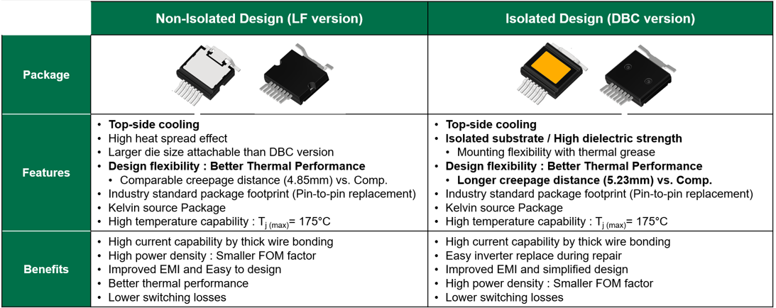
With an industry-standard footprint of 14mm x 18.58mm, the TSPAK packages provide superior thermal performance and Kelvin source configuration to minimizes gate noise and reduces turn-on losses by 60%, enabling higher-frequency operation and improved power density.
The PCR120N40M2A (LF version) and PCRZ120N40M2A (DBC version) are automotive-grade 1200V/40mΩ eSiC MOSFETs in TSPAK packages, leveraging Power Master Semiconductor’s 2nd-generation eSiC MOSFET technology to deliver optimized performance for the automotive systems.
- E-compressors, vital for efficient thermal management, extended battery life, enhanced charging efficiency, and improved driving range.
- Totem-Pole PFC and CLLC/DAB (Dual Active Bridge) topologies, essential for bidirectional power conversion in 800V battery systems used in electric vehicles.
“Cooling is one of the greatest challenges in high power design and successfully addressing it is the key enabler to reducing size and weight, which is critical in modern automotive design” said Namjin Kim, Senior Director of Sales & Marketing. “Our new top-side cooling package offer better system efficiency and minimize heat thermal path on the PCB, the system design will be simplified and compacted. We are confident that this innovative solution will be the optimal choice for high-performance automotive applications.”
“Efficient cooling is a critical challenge for reducing size and weight of high-power automotive systems,” said Namjin Kim, Senior Director of Sales & Marketing. “Our new top-side cooling package enhances system efficiency and minimizes the thermal path on the PCB, enabling simpler, more compact system designs. We believe this innovative solution will drive the high performance automotive applications.”
Original – Power Master Semiconductor
-

DENSO Corporation and Fuji Electric Co., Ltd. announced that a semiconductor supply plan submitted jointly by the companies has been approved by the Ministry of Economy, Trade and Industry. Under this plan, the companies will take part in joint investment and production of silicon carbide (SiC) power semiconductors to develop and strengthen frameworks for the supply of said semiconductors.
Power semiconductors are vital to the efficient supply of electric power. Demand for power semiconductors has been rising rapidly given that they are used in electrified vehicles, which are being adopted at an accelerated pace amid the push for the decarbonization of society. In comparison to prior silicon semiconductors, SiC power semiconductors are able to deliver superior performance under high temperature, high-frequency, and high-voltage conditions.
These devices are therefore anticipated to make large contributions to reductions in power loses as well as to more compact and lighter-weight designs for battery electric vehicle systems and other power electronics. Accordingly, growth in demand is projected for SiC power semiconductors.
In response to electrification trends, DENSO has advanced SiC technology development projects targeting increased quality and efficiency in relation to everything from wafers and element devices to modules and inverters. Meanwhile, Fuji Electric has constructed extensive frameworks encompassing all tasks spanning from the development of SiC power semiconductor elements that enable increased efficiency and more compact designs for power electronics equipment to mass production of the related modules.
Based on the approved plan, these companies will combine their respective automotive product development and production technology capabilities in a joint effort to expand their capacity for the efficient and stable supply of SiC power semiconductors throughout Japan.
Through this partnership, the companies will contribute to the development of semiconductor supply frameworks within Japan and to the improvement of the international competitiveness of Japan’s domestic semiconductor and automotive industries. In addition, this partnership is anticipated to help advance the decarbonization of society.
Original – Fuji Electric
-
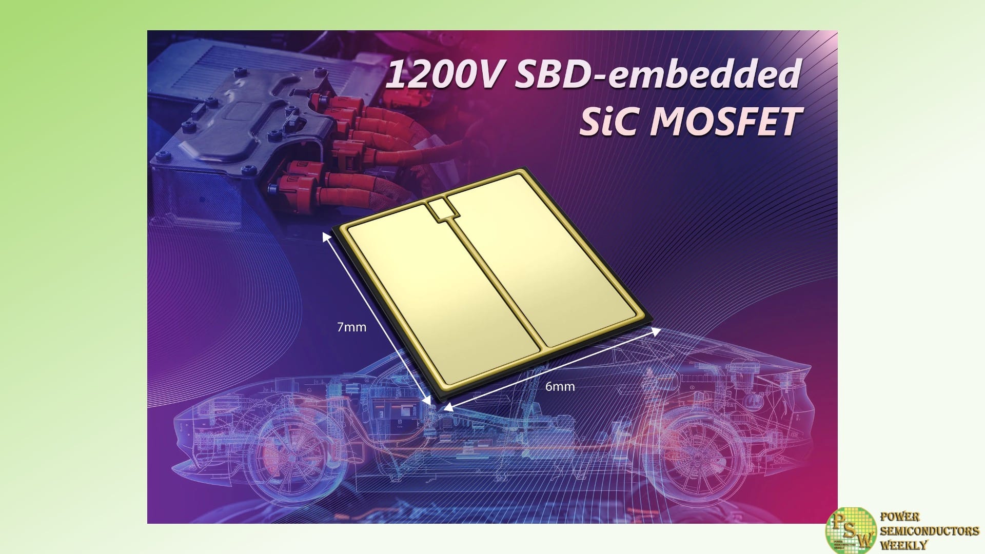
Toshiba Electronics Europe GmbH has developed new 1200V silicon carbide (SiC) MOSFETs with low on-resistance (RDS(ON)) and high levels of reliability. The devices are particularly suited to applications within automotive traction inverters. They are now available and shipping as early test samples in bare die format – allowing customers to customise them to meet the needs of their applications.
The new X5M007E120 uses a manufacturing process that reduces on-resistance per unit area by up to 30%. Unlike existing methods that utilise a striped-pattern construction, the new devices arrange the embedded Schottky barrier diodes (SBDs) in a check-pattern to achieve lower on-resistance.
Many SiC MOSFETs increase on-resistance as body diodes are energised during reverse conduction, which can lead to reliability issues. Toshiba SiC MOSFETs alleviate this issue by preventing body diodes from operating as SBDs are embedded into the MOSFETs. This approach maintains the reduction in on-resistance while ensuring reliability during reverse conduction.
With electric motors consuming over 40% of the world’s electrical energy, efficient operation is essential to sustainability. The re-arrangement of SBDs in this device has suppressed body diode energisation, and the upper limit of unipolar operation has increased to around double without increasing the SBD mounting area. Additionally, channel density is improved. These enhancements contribute to energy efficiency in applications, including motor control inverters.
Reducing RDS(ON) within a SiC MOSFET can cause excess current flow during short-circuit operations. By adopting a deep barrier structure, the X5M007E120 reduces excessive current within the MOSFET section and leakage current in the SBDs section during short-circuit operation. This enables durability during short-circuit conditions while maintaining high levels of reliability against reverse conduction operation.
The new X5M007E120 has a VDSS of 1200V and is rated for a drain current (ID) of 229A continuously, with 458A for pulsed operation (ID Pulse). RDS(ON) is as low as 7.2mΩ, and the device can operate with channel temperatures (Tch) as high as 175°C. The devices are AEC-Q100 qualified for automotive applications.
Engineering samples of the new X5M007E120 are expected to ship during 2025, with mass production samples scheduled to start in 2026.
Toshiba will continue to seek ways to further improve the characteristics of its products. The company will contribute to realising a decarbonised society by providing customers with power semiconductors for applications where energy efficiency is essential, such as inverters for motor control and power control systems for electrical vehicles.
Original – Toshiba
-
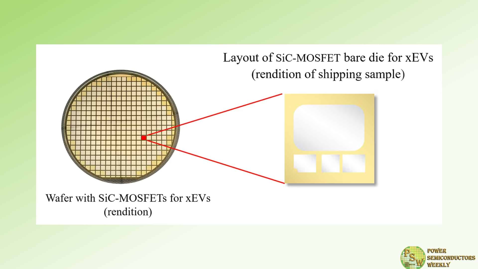
Mitsubishi Electric Corporation announced that it will begin shipping samples of a silicon carbide (SiC) metal-oxide-semiconductor field-effect transistor (MOSFET) bare die for use in drive-motor inverters of electric vehicles (EVs), plug-in hybrid vehicles (PHEVs) and other electric vehicles (xEVs) on November 14.
Mitsubishi Electric’s first standard-specification SiC-MOSFET power semiconductor chip will enable the company to respond to the diversification of inverters for xEVs and contribute to the growing popularity of these vehicles. The new SiC-MOSFET bare die for xEVs combines a proprietary chip structure and manufacturing technologies to contribute to decarbonization by enhancing inverter performance, extending driving range and improving energy efficiency in xEVs.
Mitsubishi Electric’s new power semiconductor chip is a proprietary trench SiC-MOSFET that reduces power loss by about 50% compared to conventional planar SiC-MOSFETs. Thanks to proprietary manufacturing technologies, such as a gate oxide film process that suppresses fluctuations in power loss and on-resistance, the new chip achieves long-term stability to contribute to inverter durability and xEV performance.
Original – Mitsubishi Electric
