-

Cambridge GaN Devices (CGD) is exhibiting at the prestigious IEEE Energy Conversion Congress and Expo on Booth 319. Now in its 16th year, ECCE 2024 is sponsored by both the IEEE Industrial Application Society (IAS) and IEEE Power Electronics Society (PELS). The event continues to grow, both in attendance and content.
ECCE 2024 will feature two-page Late Break Research Briefs, Post-Journal paper presentations, and the standard technical papers. It will also offer special sessions on emerging technologies and industry-oriented topics, and of course, tutorials, which have become a staple element of the ECCE technical program.
Andrea Bricconi | Chief Marketing Officer, CGD
“It is important for CGD that we spread our message that GaN is the future of power electronics, in terms of energy efficiency, power density and smallest carbon footprint, and that our ICeGaN® GaN power ICs are the most rugged and easiest-to-use devices available. Therefore we are delighted to exhibit for the first time at ECCE.”
At the event, CGD will show a number of demos that employ ICeGaN, including:
- 3 kW PFC reference design
- QORVO motor drive evaluation kit developed in partnership with CGD and utilising ICeGaN
- Slim 100W adaptor
- Half-bridge, full-bridge as well as ICeGaN in parallel evaluation boards
- 300W PFC+LLC
- Single leg of a 3-phase automotive inverter demo board, developed in partnership with French public R&I institute, IFP Energies nouvelles (IFPEN)
- ICeGaN vs discrete GaN circuits comparison in half bridge (daughter cards) demo board
Original – Cambridge GaN Devices
-

Navitas Semiconductor announced GaNSlim™, a new generation of highly-integrated GaN power ICs that will further simplify and speed the development of small form factor, high-power-density applications by offering the highest level of integration and thermal performance.
GaNSlim enables the simplest, fastest, and smallest system design by integrating drive, control, and protection, with integrated EMI control and loss-less current sensing, all within a high thermal performance proprietary DPAK-4L package. Additionally, with an ultra-low startup current below 10 µA, GaNSlim devices are compatible with industry-standard SOT23-6 controllers and eliminate HV startup.
Integrated features such as loss-less current sensing eliminate external current sensing resistors and optimize system efficiency and reliability. Over-temperature protection ensures system robustness and auto sleep-mode increases light and no-load efficiency. Autonomous turn-on/off slew rate control maximizes efficiency and power density while reducing external component count, system cost and EMI.
GaNSlim features a patented, 4-pin, high-thermal-performance, low-profile, low-inductance, DPAK package. This package enables 7 °C lower temperature operation versus conventional alternatives, supporting high-power-density designs with ratings up to 500 W. Target applications include chargers for mobile devices and laptops, TV power supplies, lighting, etc.
“Our GaN focus is on integrated devices that enable high-efficiency, high-performance power conversion with the simplest designs and the shortest possible time-to-market,” says Reyn Zhan, Sr. Manager of Technical Marketing. “Our new GaNSlim portfolio – built on integration, ease-of-use, and low-cost manufacturing methods, – continues to grow the customer pipeline with over 50 new projects already identified. GaNSlim increases our GaN addressable market by enabling lower system costs compared to silicon designs for many applications, targeting applications under 500 W across mobile, consumer and home appliance.”
Devices in the NV614x GaNSlim family are rated at 700 V with RDS(ON) ratings from 120 mΩ to 330 mΩ and are available in versions optimized for both isolated and non-isolated topologies.
As with other Navitas GaN ICs, GaNSlim devices are supplied with an industry-leading twenty-year warranty, while demo boards for QR flyback, single-stage PFC, boost PFC plus QR flyback and TV power supply designs allow for rapid evaluation and selection of the optimum device for a given application.
Original – Navitas Semiconductor
-

Infineon Technologies AG announced a partnership with Canada-based AWL-Electricity Inc., a pioneer in MHz resonant capacitive coupling power transfer technology. Infineon provides AWL-E with CoolGaN™ GS61008P allowing the development of advanced wireless power solutions, enabling new ways to solve power challenges in various industries.
The partnership combines Infineon’s cutting-edge gallium nitride (GaN) technology with AWL-E’s innovative MHz resonant capacitive coupling power transfer system, achieving industry-benchmark wireless power efficiencies. Infineon’s GaN transistor technology offers highest efficiency and highest power density while operating at highest switching frequencies.
This enables AWL-E to increase its system lifetime, reduces downtime and operating costs, and improves ease-of-use for consumers. In the automotive sector, the technology enables a new level of interior experiences and seat dynamics. In industrial systems, it provides near-unconstrained levels of design freedom, such as for automated guided vehicles or robotic applications. Additionally, the technology allows for a fully sealed system design, eliminating the need for charging ports which contributes to reducing global consumption of batteries.
“With our partner approach we prove once more the ability to unlocking the full system-level benefits of Infineon’s CoolGaN technology, enabling compactness and efficiency,” said Falk Herm, Global Partnership & Ecosystem Management at Infineon’s Power & Sensor Systems (PSS) Division at Infineon. “The combination of AWL-E and Infineon’s complementary capabilities demonstrates how the features of GaN, namely operating at MHz frequencies, change the paradigm of what can be done with power transistors, driving greener and better performing products.”
“Infineon uniquely brings you into their family with a recognition that a strong ecosystem ultimately solves today’s power needs,” said Francis Beauchamp-Verdon, Co-founder, VP and Business Development Director at AWL-E. “Infineon’s GaN transistors, eval boards, and partner opportunities have boosted acceptance of our GaN-based MHz power coupling systems.”
Infineon is a leader in the power semiconductor market and currently the only manufacturer mastering all power technologies while offering the broadest product and technology portfolio of silicon (such as SJ MOSFETs, IGBTs), silicon carbide (such as Schottky diodes and MOSFETs) and gallium-nitride-based (e-mode HEMT) devices, covering bare die, discretes, and modules.
Original – Infineon Technologies
-

Navitas Semiconductor announced that its high-power GaNSafe family is now available in a TOLT (Transistor Outline Leaded Top-side cooling) package.
The GaNSafe family has been specifically created to serve demanding, high-power applications, such as AI data centers, solar/energy storage, and industrial markets. Navitas 4th generation integrates control, drive, sensing, and critical protection features that enable unprecedented reliability and robustness. GaNSafe is the world’s safest GaN with short-circuit protection (350ns max latency), 2kV ESD protection on all pins, elimination of negative gate drive, and programmable slew rate control. All these features are controlled with 4-pins, allowing the package to be treated like a discrete GaN FET, requiring no VCC pin.
The TOLT packaging enhances thermal dissipation through the top side of the package, allowing heat to be dissipated directly to the heatsink (not through the PCBA). This enables the reduction of operating temperature and increases current capability, resulting in the highest level of system power density, efficiency, and reliability.
“With over 200 million units shipped and supplied with a 20-year warranty, Navitas’ highly integrated high-power GaNSafe ICs are proven to deliver performance and reliability while simplifying Design-IN for systems up to 22kW,” says Charles Bailley, Senior Director of Business Development. “As the most protected, reliable, and safe GaN devices in the industry, GaNSafe took our technology into mainstream applications above 1kW. Now, with the enhanced thermal dissipation of the TOLT package, we are enabling customers to deliver even better performance, efficiency, power density, and reliability in even the most demanding applications.”
Suitable for applications from 1 kW to 22 kW, 650 V GaNSafe in TOLT packaging is available with a range of RDS(ON)MAX from 25 to 98 mΩ. Integrated features and functions include:
- High-speed short-circuit protection, with autonomous ‘detect and protect’ with ultra-fast 350 ns / 50 ns latency.
- Protected, regulated, integrated gate-drive control, with zero gate-source loop inductance for reliable high-speed 2 MHz switching capability to maximize application power density.
- Electrostatic discharge (ESD) protection of 2 kV, compared to zero for discrete GaN transistors.
- 650 V continuous, and 800 V transient voltage capability for extraordinary application conditions.
- Integrated Miller Clamp (no negative gate bias, higher 3rd quadrant efficiency)
- Programmable turn-on and turn-off speeds (dV/dt) to simplify EMI regulatory requirements.
- Simple 4-pin device, allowing the package to be treated like a discrete GaN and requiring no additional VCC pin
- Robust, thermally enhanced packaging: ultra-low RQ_JUNC-AMB and board-level thermal cycling (BLTC) Reliability
In addition to the new ICs, Navitas will be offering reference design platforms based on GaNSafe TOLT for applications including data center power supplies and EV on-board chargers. These system platforms include complete design collateral with fully tested hardware, embedded software, schematics, bill-of-materials, layout, simulation, and hardware test results.
Original – Navitas Semiconductor
-

CISSOID announced that its SiC Inverter Control Module (ICM) has been adopted by Hydro Leduc, a renowned manufacturer of hydraulic components, for its new highly efficient and modular Electric Power Take-Off (ePTO). This new ePTO solution supports the electrification of trucks and other off-road vehicles. CISSOID’s ICM not only powers and controls Hydro Leduc’s compact and efficient inverter but also contributed to greatly accelerate its development cycle.
Hydro Leduc’s new ePTO solution offers an optimized hydraulic supply to high power tools in e-trucks and other off-road vehicles that remain driven by hydraulic actuators. Hydro Leduc’s new ePTO represents a significant advancement in electric and hydraulic transmissions with their ME230, a 76 kW brushless electric motor designed to be paired with an inverter for applications up to 650Vdc.
This motor, compatible with DIN ISO14 standards and equipped with an efficient cooling system, forms a complete solution with the new series of fixed displacement spherical piston pumps: the XRe, available in 41 or 63 cm³ displacements.
Specially adapted for E-PTO mounting, the XRe series is quiet and offers remarkable efficiency, reduced pulsations due to its 9-piston design, and high speed in self-priming mode. Together, the ME230 and XRe provide high-performance and efficient electro-hydraulic solutions for a variety of applications.
CISSOID’s ICM optimally integrates a 3-Phase 1200V/340A-550A SiC Power Module, enabling efficient power conversion, a gate driver board designed for safe driving of the fast-switching SiC transistors, and a control board embedding a powerful real-time microprocessor. This hardware platform has been delivered together with the OLEA® APP INVERTER software optimized for the efficient and safe control of electric motors.
Olivier Savinois, Managing Director at EL MOTION (the sister company of Hydro Leduc, specialized in the design and manufacturing of electrical components and motors), said “We have been very pleased to work with CISSOID on the development of our new ePTO inverter. Not only did their SiC Inverter Control Module completely match our needs, we also enjoyed outstanding support from their team. Especially due to the on-site calibration of our inverter and motor, during the design and validation phases. CISSOID’s modular inverter platform ties perfectly with our scalable ePTO solution.”
Emmanuel Poli, VP Sales at CISSOID, said: “It was really exciting to work with the Hydro Leduc team, who rapidly understood how powerful it would be to leverage our ICM to accelerate the design of their inverter. We were impressed by the speed and agility of Hydro Leduc’s engineers in integrating our hardware and software solution into their motor drive.”
Original – CISSOID
-
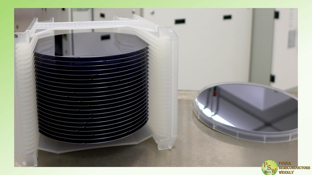
Coherent Corp. announced the launch of its 200 mm silicon carbide epitaxial wafers. Substrate and epi-wafer shipments from the company at 350 micron and 500 micron thickness are now underway.
As a dedicated manufacturer of both SiC substrates and epitaxial wafers, Coherent combines these elements to deliver exceptional quality, performance, and reliability. The new 200 mm SiC epi-wafers are engineered with cutting-edge thickness and doping uniformity, setting new industry standards and supporting the production of superior SiC power semiconductors.
“With our advanced technology, we are not only enhancing the quality of SiC devices but also addressing the growing demand for 200 mm for efficient power-conversion components in critical sectors,” said Gary Ruland, Vice President and General Manager of the SiC Materials Business Unit.
SiC devices are integral to power conversion in electric and hybrid vehicles, energy infrastructure, and high-power EV chargers. The transition from 150 mm to 200 mm diameter wafers responds to the increasing demand for SiC semiconductors, allowing manufacturers to produce more devices per wafer. This shift is expected to enhance productivity and reduce the cost of SiC devices, benefiting a wide range of applications.
By adopting larger wafers, SiC device manufacturers can achieve higher yields and improved cost efficiency because of a 1.8x increase in usable area per wafer. The implementation of state-of-the-art 200 mm tooling brings additional advantages while aligning with the industry’s drive for greater performance and reduced operational costs.
Original – Coherent
-
 LATEST NEWS / PRODUCT & TECHNOLOGY / SiC / WBG
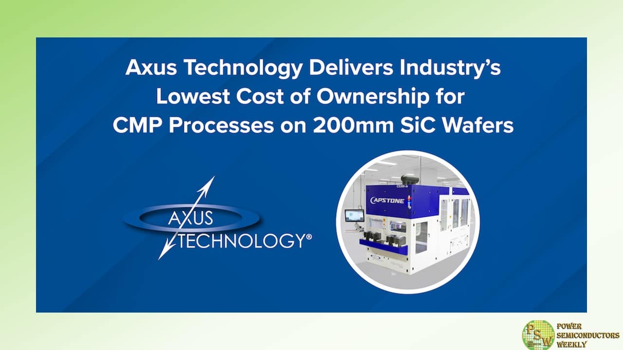
Axus Technology Introduced Industry’s Lowest Cost of Ownership for CMP Processes on 200mm SiC Wafers
September 26, 2024
2 Min ReadAxus Technology, a leading global provider of chemical mechanical planarization (CMP) equipment, critical for semiconductor and compound semiconductor fabrication, announced its flagship CapstoneÆ CS200 platform tools offer the industry’s lowest cost of ownership (CoO) for CMP processes on 200mm silicon carbide (SiC) wafers. Compared to its closest competitor, Axus’s small-footprint Capstone delivers twice the throughput at less than half the total cost per wafer.
Yole Group forecasts the overall SiC manufacturing tool market to top US$4.4 billion by 2029. “The unique properties of SiC require specialized manufacturing tools and lines for processing power SiC devices,” the market analyst firm noted earlier this year. Axus anticipated this need, designing the state-of-the-art Capstone from the ground up to deliver advanced processing capabilities for SiC in power electronics and other applications.
“Many 200mm fabs are looking to upgrade their installed base of CMP tools to products with leading-edge capability and functionality. Our ability to deliver industry-low CoO further underscores our strong market position and capacity to support this shift,” said Axus Technology CEO Dan Trojan. “Capstone features a streamlined workflow and integrated cleaning capability, so it requires half the process steps of older CMP tools. This allows customers to greatly lower their capex investment.”
Key Capstone CoO advantages vs. competitor
- Throughput: 2.5x wafers per hour
- Power consumption: 60% lower
- DI water consumption: 80% lower
- Footprint: 45% smaller
- Capex cost per wafer: 65% lower
- Total cost per wafer: 50% lower
Another factor contributing to Capstone’s lower CoO is its built-in Process Temperature Control (PTC) technology, which enables processing at higher pressures and speeds without exceeding temperature limits of polishing pads and other sensitive components. This feature is vital for SiC and other materials with high hardness and planarization challenges that necessitate more aggressive process conditions.
Axus built its proprietary CoO model using its own system specifications, publicly available specs for competitive tools, actual consumables costs, and real-world performance data supplied by customers. The comprehensive model factors in all CoO contributors: process variables (polish time and removal rates), polishing and cleaning consumables, power and deionized (DI) water usage, system footprint, and equipment capex including cost, utilization and wafer capacity.
Original – Axus Technology
-
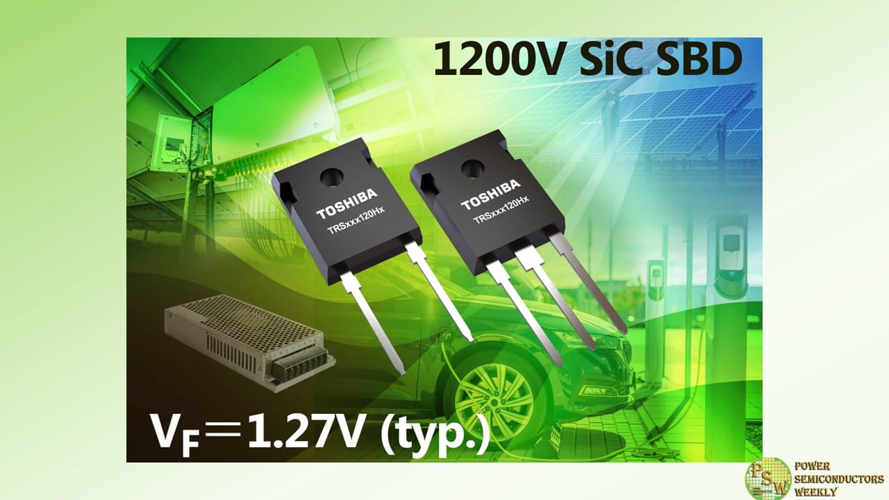
Toshiba Electronics Europe GmbH enhances its silicon carbide (SiC) diode portfolio with ten new 1200V Schottky barrier diodes (SBDs). The TRSxxx120Hx series, comprising five products housed in TO-247-2L packages and five in TO-247 packages, helps designers improve the efficiency of industrial equipment, including photovoltaic (PV) inverters, electric vehicle (EV) charging stations, and switching power supplies.
By implementing an enhanced junction barrier Schottky (JBS) structure, the TRSxxx120Hx series allows a very low forward voltage (VF) of just 1.27V (typ.). The merged PiN-Schottky incorporated into a JBS structure reduces diode losses under high current conditions. The TRS40N120H of the new series accepts a forward DC current (IF(DC)) of 40A (max) and a non-repetitive peak forward surge current (IFSM) of 270A (max), with the maximum case temperature (TC) of all devices being +175°C.
Combined with the lower capacitive charge and leakage current, the products help improve system efficiency and simplify thermal design. For instance, at a reverse voltage (VR) of 1200V, the TRS20H120H diode housed in the TO-247-2L package provides a total capacitive charge (QC) of 109nC and reverse current (IR) of 2µA.
Original – Toshiba
-
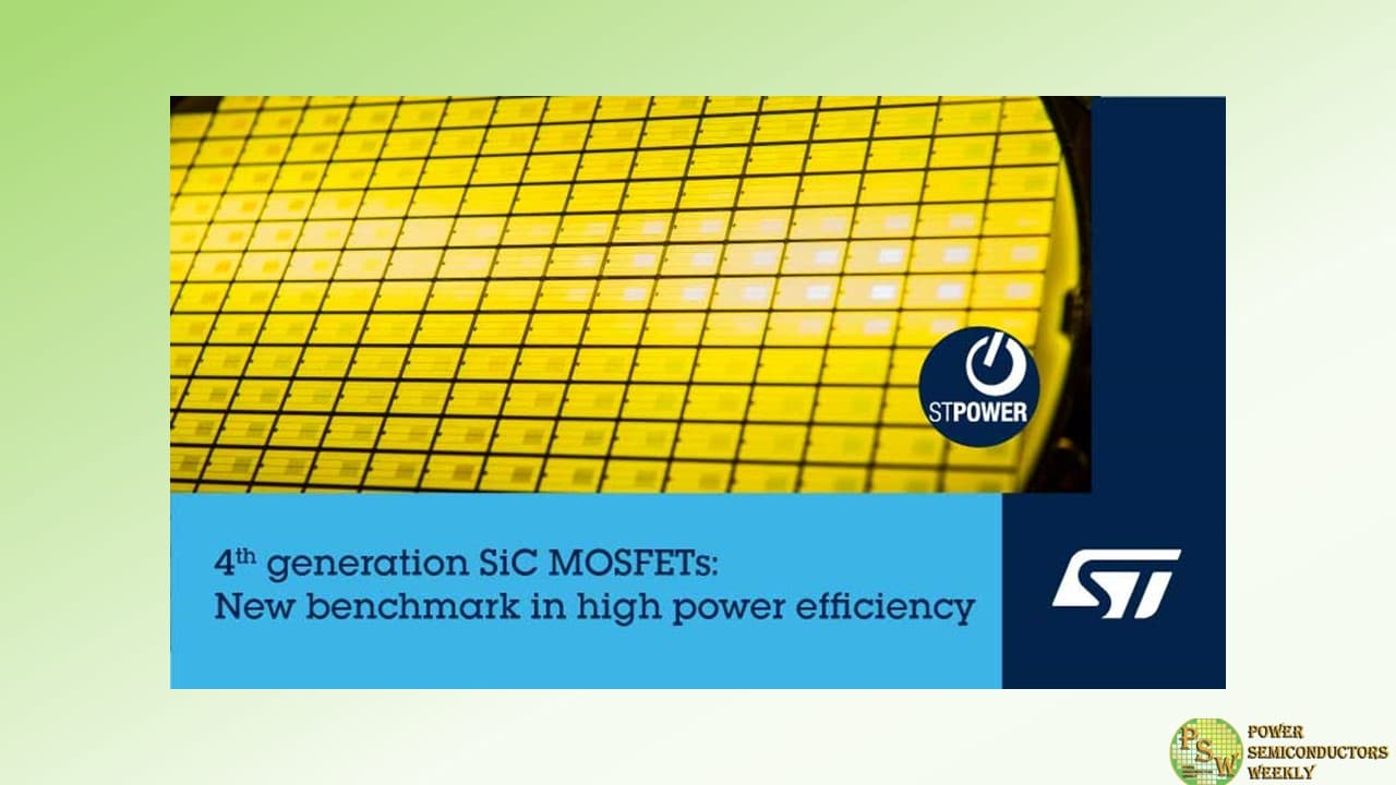
STMicroelectronics introduced its fourth generation STPOWER silicon carbide (SiC) MOSFET technology. The Generation 4 technology brings new benchmarks in power efficiency, power density and robustness. While serving the needs of both the automotive and industrial markets, the new technology is particularly optimized for traction inverters, the key component of electric vehicle (EV) powertrains. The company plans to introduce further advanced SiC technology innovations through 2027 as a commitment to innovation.
“STMicroelectronics is committed to driving the future of electric mobility and industrial efficiency through our cutting-edge silicon carbide technology. We continue to advance SiC MOSFET technology with innovations in the device, advanced packages, and power modules,” said Marco Cassis, President, Analog, Power & Discrete, MEMS and Sensors Group. “Together with our vertically integrated manufacturing strategy, we are delivering industry leading SiC technology performance and a resilient supply chain to meet the growing needs of our customers and contribute to a more sustainable future.”
As the market leader in SiC power MOSFETs, ST is driving further innovation to exploit SiC’s higher efficiency and greater power density compared to silicon devices. This latest generation of SiC devices is conceived to benefit future EV traction inverter platforms, with further advances in size and energy-saving potential. While the EV market continues to grow, challenges remain to achieve widespread adoption and car makers are looking to deliver more affordable electric cars.
800V EV bus drive systems based on SiC have enabled faster charging and reduced EV weight, allowing car makers to produce vehicles with longer driving ranges for premium models. ST’s new SiC MOSFET devices, which will be made available in 750V and 1200V classes, will improve energy efficiency and performance of both 400V and 800V EV bus traction inverters, bringing the advantages of SiC to mid-size and compact EVs — key segments to help achieve mass market adoption.
The new generation SiC technology is also suitable for a variety of high-power industrial applications, including solar inverters, energy storage solutions and datacenters, significantly improving energy efficiency for these growing applications.
ST has completed qualification of the 750V class of the fourth generation SiC technology platform and expects to complete qualification of the 1200V class in the first quarter of 2025. Commercial availability of devices with nominal voltage ratings of 750V and 1200V will follow, allowing designers to address applications operating from standard AC-line voltages up to high-voltage EV batteries and chargers.
ST’s Generation 4 SiC MOSFETs provide higher efficiency, smaller components, reduced weight, and extended driving range compared to silicon-based solutions. These benefits are critical for achieving widespread adoption of EVs and leading EV manufacturers are engaged with ST to introduce the Generation 4 SiC technology into their vehicles, enhancing performance and energy efficiency. While the primary application is EV traction inverters, ST’s Generation 4 SiC MOSFETs are also suitable for use in high-power industrial motor drives, benefiting from the devices’ improved switching performance and robustness.
This results in more efficient and reliable motor control, reducing energy consumption and operational costs in industrial settings. In renewable energy applications, the Generation 4 SiC MOSFETs enhance the efficiency of solar inverters and energy storage systems, contributing to more sustainable and cost-effective energy solutions. Additionally, these SiC MOSFETs can be utilized in power supply units for server datacenters for AI, where their high efficiency and compact size are crucial for the significant power demands and thermal management challenges.
To accelerate the development of SiC power devices through its vertically integrated manufacturing strategy, ST is developing multiple SiC technology innovations in parallel to advance power device technologies over the next three years. The fifth generation of ST SiC power devices will feature an innovative high-power density technology based on planar structure. ST is at the same time developing a radical innovation that promises outstanding on-resistance RDS(on) value at high temperatures and further RDS(on) reduction, compared to existing SiC technologies.
ST will attend ICSCRM 2024, the annual scientific and industry conference exploring the newest achievements in SiC and other wide bandgap semiconductors. The event, from September 29 to October 04, 2024, in Raleigh, North Carolina will include ST technical presentations and an industrial keynote on ‘High volume industrial environment for leading edge technologies in SiC’.
Original – STMicroelectronics
-
Resonac Corporation (formerly Showa Denko K.K.) and Soitec have signed an agreement to develop 200mm (8-inch) SmartSiC™ silicon carbide (SiC) wafers using Resonac substrates and epitaxy processes, in a major step for the deployment of Soitec’s high-yielding silicon carbide technology in Japan and other international markets.
SmartSiC™ silicon carbide is a disruptive compound semiconductor material providing superior performance and efficiency over silicon in high-growth power applications for electric mobility and industrial processes. It allows for more efficient power conversion, lighter and more compact designs and overall system cost savings – all key factors for success in automotive and industrial systems.
Christophe Maleville, Chief Technology Officer at Soitec, commented: “Silicon carbide is beingadopted for EV and industrial applications, where it brings a significant system cost advantage. To further accelerate this adoption, silicon carbide yield and productivity must be improved. Associating Resonac premium quality SiC materials with Soitec’s unique 200mm (8-inch) SmartSiC™ technology will support volume availability of record quality epi-ready substrate. The combination of our respective technologies and products will optimize these substrates using Resonac’s high-quality epitaxy. Soitec is proud and excited to be partnering with Resonac to develop a best-in-class combined SiC product offering for Japan and the world.”
Makoto Takeda, General Manager of Device Solutions Business Unit at Resonac, commented: “We are delighted to announce this partnership with Soitec, which is fully aligned with our broader commitment to sustainable and energy-efficient semiconductor solutions. By combining Resonac’s high quality monocrystalline silicon carbide wafers with Soitec’s unique SmartSiC™ technology, we will deliver improved production efficiency of 200mm (8-inch) silicon carbide wafers and diversify the epi-wafer supply chain.”
Soitec’s SmartSiC™ silicon carbide wafers, or engineered substrates, are produced using the company’s proprietary SmartCut™ technology to bond an ultra-fine layer of high-quality monoSiC ‘donor’ wafer to a low-resistivity polycrystalline (poly-SiC) ‘handle’ wafer. The resulting engineered substrate delivers significantly improved device performance and manufacturing yields. By allowing multiple re-uses of the prime quality mono-SiC wafer, the process also reduces overall energy consumption during wafer manufacturing.
Soitec has a new fabrication plant at its headquarters in Bernin, France, primarily dedicated to the production of SmartSiC™ wafers for electric vehicles, renewable energy and industrial equipment component applications.
Original – Soitec
