-

Axcelis Technologies, Inc. will be participating in the International Conference on Silicon Carbide and Related Materials (ICSCRM 2024) taking place September 29 – October 4, 2024, at the Raleigh Convention Center in North Carolina. At the event, Axcelis’ management will be available for one-on-one meetings.
President and CEO of Axcelis, Dr. Russell Low: “We’re excited to participate in ICSCRM 2024, one of the most important technology forums in the power market. Axcelis’ Purion™ Power Series is the technology leader in this market, due to its enabling and highly differentiated features and process control. Ion implant is one of the most critical steps in the manufacturing of Silicon Carbide devices, a market which is estimated by Yole to grow at a 25% CAGR from 2023 – 2029.”
Original – Axcelis Technologies
-
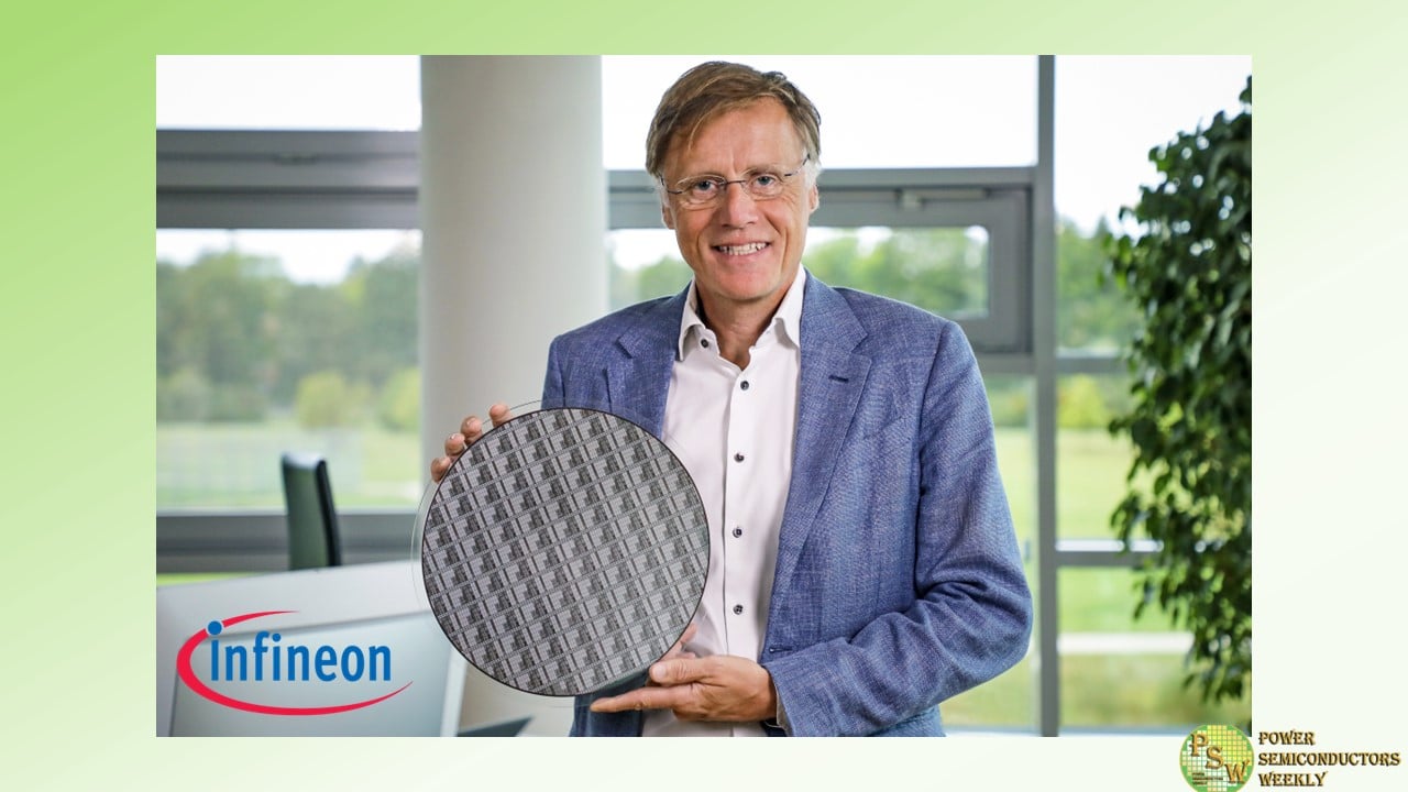
Infineon Technologies AG announced that the company has succeeded in developing the world’s first 300 mm power gallium nitride (GaN) wafer technology. Infineon is the first company in the world to master this groundbreaking technology in an existing and scalable high-volume manufacturing environment. The breakthrough will help substantially drive the market for GaN-based power semiconductors.
Chip production on 300 mm wafers is technologically more advanced and significantly more efficient compared to 200 mm wafers, since the bigger wafer diameter fits 2.3 times as many chips per wafer.
GaN-based power semiconductors find fast adoption in industrial, automotive, and consumer, computing & communication applications, including power supplies for AI systems, solar inverters, chargers and adapters, and motor-control systems. State-of-the art GaN manufacturing processes lead to improved device performance resulting in benefits in end customers’ applications as it enables efficiency performance, smaller size, lighter weight, and lower overall cost. Furthermore, 300 mm manufacturing ensures superior customer supply stability through scalability.
“This remarkable success is the result of our innovative strength and the dedicated work of our global team to demonstrate our position as the innovation leader in GaN and power systems,” said Jochen Hanebeck, CEO of Infineon Technologies AG. “The technological breakthrough will be an industry game-changer and enable us to unlock the full potential of gallium nitride. Nearly one year after the acquisition of GaN Systems, we are demonstrating again that we are determined to be a leader in the fast-growing GaN market. As a leader in power systems, Infineon is mastering all three relevant materials: silicon, silicon carbide and gallium nitride.”
Infineon has succeeded in manufacturing 300 mm GaN wafers on an integrated pilot line in existing 300 mm silicon production in its power fab in Villach (Austria). The company is leveraging well-established competence in the existing production of 300 mm silicon and 200 mm GaN. Infineon will further scale GaN capacity aligned with market needs. 300 mm GaN manufacturing will put Infineon in a position to shape the growing GaN market which is estimated to reach several billion US-Dollars by the end of the decade.
This pioneering technological success underlines Infineon’s position as a global semiconductor leader in power systems and IoT. Infineon is implementing 300 mm GaN to strengthen existing and enabling new solutions and application fields with an increasingly cost-effective value proposition and the ability to address the full range of customer systems. Infineon will present the first 300 mm GaN wafers to the public at the electronica trade show in November 2024 in Munich.
A significant advantage of 300 mm GaN technology is that it can utilize existing 300 mm silicon manufacturing equipment, since gallium nitride and silicon are very similar in manufacturing processes. Infineon’s existing high-volume silicon 300 mm production lines are ideal to pilot reliable GaN technology, allowing accelerated implementation and efficient use of capital. Fully scaled 300 mm GaN production will contribute to GaN cost parity with silicon on R DS(on) level, which means cost parity for comparable Si and GaN products.
300 mm GaN is another milestone in Infineon’s strategic innovation leadership and supports Infineon’s mission of decarbonization and digitalization.
Original – Infineon Technologies
-
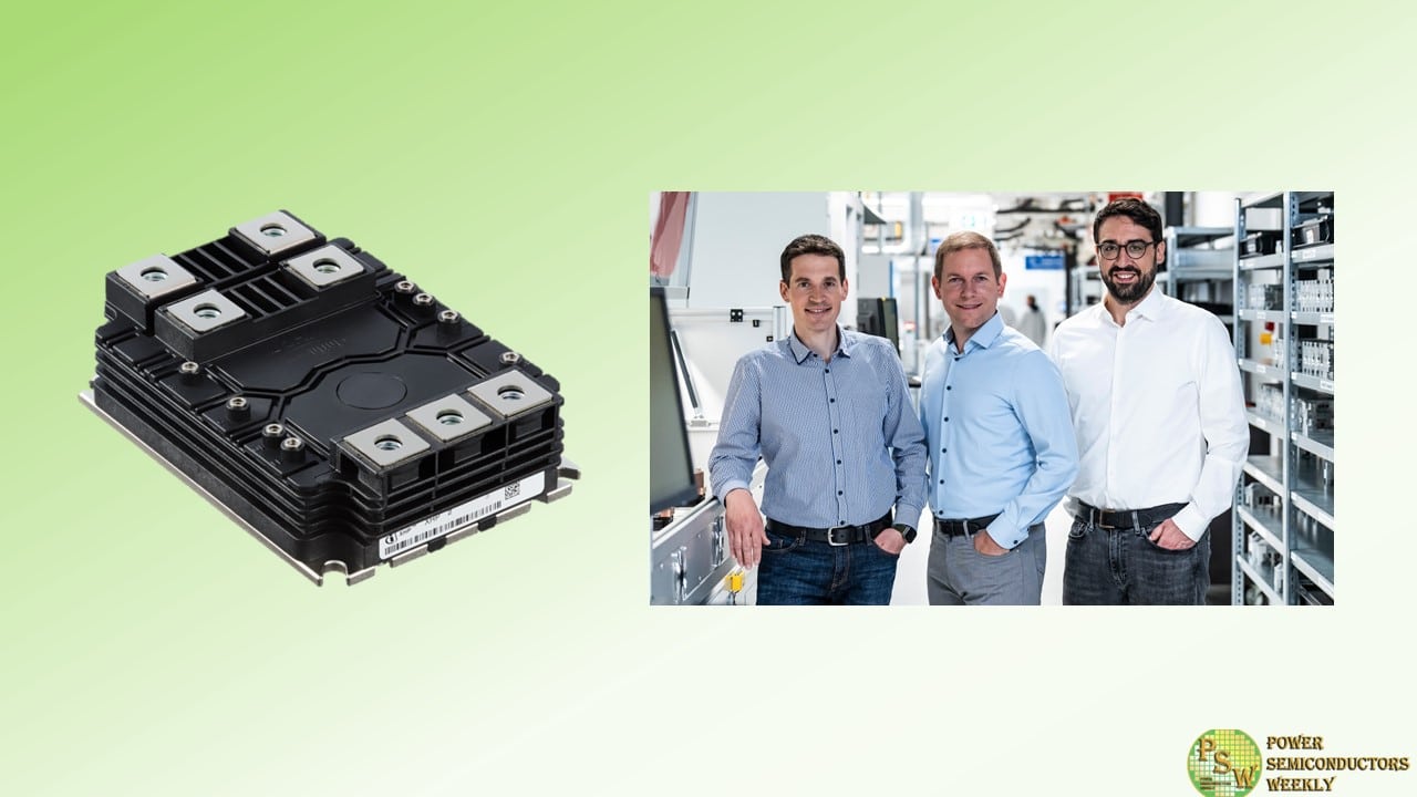
Infineon Technologies AG has been nominated for the Deutscher Zukunftspreis 2024, the Federal President’s Award for Technology and Innovation, for its development of a new type of energy-saving chip based on the innovative semiconductor material silicon carbide (SiC). The Jury of Deutscher Zukunftspreis has announced the three nominated teams in Munich.
A team of developers from Infineon, together with Chemnitz University of Technology, has succeeded in developing the world’s first silicon carbide MOSFET with a vertical channel (trench MOSFET) and innovative copper contacting in the 3300V voltage class. The new SiC modules and the power converters equipped with the modules represent a revolutionary innovation leap in semiconductor technology from conventional silicon to more energy-efficient silicon carbide, which reduces switching losses in high-current applications by 90%.
MOSFETs are electrical switches for a wide range of applications. Trench MOSFETs differ from so-called planar MOSFETs in their cell structure and performance. While the current flow in planar MOSFETs is initially horizontal, trench MOSFETs offer purely vertical channels. This results in a higher cell density per surface area, which in turn significantly reduces the losses in the chip during energy conversion and therefore increases efficiency.
“The transition towards green energy and many other pressing challenges of our time can only be solved with technological progress,” said Jochen Hanebeck, CEO of Infineon Technologies AG. “It is therefore important to promote and reward innovation and make it visible in society. The ‘Deutscher Zukunftspreis’ is the most important national award that is presented with this aim in mind. The nomination is a great honor for us and proof of the successful research and development work at Infineon. Congratulations to all colleagues involved!”
The CoolSiC™ XHP™2 module family enables significant energy savings, for example in industrial power generation in solar parks or wind turbines, in power transmission and, above all, in end consumption, where high energies in the megawatt range are required. A single train with a silicon carbide drive system can save around 300 MWh per year compared to the previous silicon-based solution. This is roughly equivalent to the annual consumption of 100 single-family homes. Together with drive technology manufacturers and rail operators, Infineon is making an important contribution to decarbonization. At the same time, local residents also benefit from the lower noise level of trains with SiC modules when they pass through residential areas.
Through numerous innovative developments in chip processing and design as well as contacting and module technology, the team led by Dr. Konrad Schraml, Dr. Caspar Leendertz (both Infineon) and Prof. Dr. Thomas Basler (Chemnitz University of Technology) has brought the 3300V CoolSiC XHP2 high-performance module to production readiness. With ten times greater reliability against thermomechanical stress and a significantly higher power density compared to silicon modules, the new silicon carbide module can also be used to electrify large drives in diesel locomotives, agricultural and construction machinery, aircraft and ships, which were previously reserved for fossil fuels. The significantly higher switching frequencies permitted by the new module are helpful, as they enable a significant reduction in weight and volume of the power converters in the application.
“This nomination shows that climate change and sustainable resource consumption have become central aspects of our society,” said Dr. Peter Wawer, Division President Green Industrial Power (GIP) at Infineon. “Innovative energy solutions and power semiconductors are a core component in decarbonization and fighting climate change, as the expert jury of Deutscher Zukunftspreis has recognized. I am proud that we at Infineon can make a significant contribution to a green future with pioneering technology.”
Project manager Dr. Konrad Schraml: “For us as a development team, it is a matter close to our hearts to develop innovative chips that contribute to efficient energy consumption and thus also to green mobility on our planet. This nomination is a great recognition for my team, whose tireless efforts, expertise and passion for sustainability have made the technology breakthrough in silicon carbide possible.”
On November 27, Federal President Frank-Walter Steinmeier presents the Deutscher Zukunftspreis to the winning team in Berlin.
Original – Infineon Technologies
-

JEDEC Solid State Technology Association announced the publication of JEP200: Test Methods for Switching Energy Loss Associated with Output Capacitance Hysteresis in Semiconductor Power Devices. Developed jointly by JEDEC’s JC-70.1 Gallium Nitride and JC-70.2 Silicon Carbide Subcommittees, JEP200 is available for free download from the JEDEC website.
Proliferation of soft switching power conversion topologies brought about the need to accurately quantify the energy stored in a power device’s output capacitance because the energy impacts efficiency of power converters. JEP200, developed in collaboration with academia, addresses the critical power supply industry need to properly test and measure the switching energy loss due to the output capacitance hysteresis in semiconductor power devices and details tests circuits, measurement methods, and data extraction algorithms. The document applies not only to wide bandgap power semiconductors such as GaN and SiC, but also silicon power transistors and diodes.
“Professionals in high-frequency power conversion systems have long sought a standardized approach to testing new switching energy losses,” said Dr. Jaume Roig, Member of Technical Staff, onsemi and Vice Chair of the JC-70 Committee. “This document now provides helpful guidance on testing energy losses related to output capacitance hysteresis caused by displacement currents. With this clarity, system optimization can proceed more accurately.”
“JEDEC’s JC-70 committee has the expertise necessary to meet the demands of the entire power semiconductor industry, and the development of JEP200 demonstrates how the JEDEC process enabled the committee to swiftly respond to an industry need,” said John Kelly, JEDEC President. “JEP200 encompasses GaN, SiC, and Si power devices, helping the industry navigate design challenges caused by the growing number of new power conversion topologies.”
Original – JEDEC
-

Wolfspeed, Inc. unveiled a silicon carbide module designed to transform the renewable energy, energy storage, and high-capacity fast-charging sectors through improved efficiency, durability, reliability, and scalability. The 2300V baseplate-less silicon carbide power modules for 1500V DC Bus applications were developed and launched utilizing Wolfspeed’s state-of-the-art 200mm silicon carbide wafers.
Wolfspeed also announced that it is partnering with EPC Power, a premier North American utility-scale inverter manufacturer. EPC Power will be employing the Wolfspeed® modules in utility-grade solar and energy storage systems, which offer a scalable high-power conversion system and high-performance controls and system redundancy.
“The solar and energy storage market remains among the fastest-growing segments of the renewable energy industry. As the pioneers of silicon carbide, we are driven to create solutions that will open the door to a new era of modern energy,” said Jay Cameron, Wolfspeed Senior Vice President and General Manager, Power. “Energy efficiency, reliability, and scalability are top of mind for our customers, such as EPC Power, who recognize the substantial advantages Wolfspeed’s silicon carbide brings to the table.”
“Silicon carbide devices open the door to a step-change in inverter performance and reliability. With our commitment to extreme reliability, performance, and security in our new ‘M’ inverter while also forging a deep commercial relationship with key suppliers, Wolfspeed was the obvious choice,” said Devin Dilley, President and Chief Product Officer, EPC Power.
With mounting global investment in renewable energy, the solar energy market is estimated to reach a $300 billion market capitalization by 2032. According to the International Energy Agency (IEA), 2024-25 will see the highest energy demand growth rate since 2007, reinforcing the need for efficient and reliable clean power. Wolfspeed’s silicon carbide solution helps bridge this crucial gap, supporting the next era of modern energy technologies while reinforcing U.S. clean energy manufacturing leadership.
Cameron continued, “This platform further validates our investments in 200mm wafer technology and production as the potential of silicon carbide continues to be recognized by industry leaders across all mission-critical applications.”
Original – Wolfspeed
-
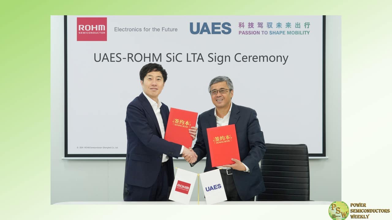
ROHM and United Automotive Electronic Systems Co., Ltd., (UAES), a leading Tier 1 automotive supplier in China, have recently entered into a long-term supply agreement for SiC power devices.
Since 2015, ROHM and UAES have been collaborating and carrying out detailed technical exchanges on automotive applications utilizing SiC power devices. This partnership deepened in 2020 with the establishment of the joint SiC technology laboratory at the UAES headquarters in Shanghai, China. And in 2021 ROHM’s advanced SiC power devices and peripheral components were highly evaluated by UAES, resulting in ROHM being selected as a preferred supplier.
The close long-standing technical partnership has led to the production and adoption of numerous automotive products equipped with ROHM SiCs, such as onboard chargers and inverters for electric vehicles. SiC power devices play a crucial role in enhancing the efficiency and performance of a variety of systems, contributing to extending the cruising range and reducing battery size.
This long-term supply agreement ensures UAES sufficient access to SiC power devices to meet the growing demand for SiC-based inverter modules, which have been supplied to customers since November 2023. Going forward, both companies will deepen their collaboration, contributing to technological innovation in the automotive sector by accelerating the development of cutting-edge SiC power solutions for EVs.
- Guo Xiaolu, Deputy General Manager, United Automotive Electronic Systems Co., Ltd.
‘The growing popularity of electric vehicles in the Chinese market has made the adoption and integration of power semiconductors like SiC increasingly important. ROHM, a world-renowned semiconductor manufacturer, is a pioneer and market leader in SiC power devices. Since 2015 we have been actively engaged in technical exchanges and highly value ROHM’s proposed solutions encompassing devices and peripheral components. Choosing ROHM as our long-term supplier of SiC chips guarantees a stable supply for future mass production. We appreciate ROHM’s past efforts and look forward to building a long-term collaborative relationship, with this agreement serving as a new starting point.’
- Tsuguki Noma, Corporate Officer and Director of the Power Device Business Unit, ROHM
‘We are very pleased to have signed a long-term supply agreement with UAES, a valued partner with whom we have built a strong cooperative relationship over the years. As a leading Tier 1 manufacturer in China, UAES is at the forefront of advanced application development. To meet the need for SiC power devices that improve efficiency in the rapidly expanding electric vehicle market, ROHM has established a leading development and manufacturing system within the SiC industry. We believe that by working together, both companies can provide cutting-edge, high performance, high quality automotive applications. Moving forward, we will continue to drive technological innovation in electric vehicles together with UAES by offering power solutions centered on SiC.’
History of Technical Collaboration Between ROHM and UAES
- 2015 Initiated technical exchange
- 2020 Established a joint SiC technology laboratory
- 2020 Began mass production of automotive products equipped with ROHM SiC power devices
- 2021 ROHM recognized as a preferred supplier for SiC power solutions
- 2024 ROHM and UAES sign a long-term supply agreement for SiC power devices
Original – ROHM
-

Navitas Semiconductor announced the release of a portfolio of third-generation automotive-qualified SiC MOSFETs in D2PAK-7L (TO-263-7) and TOLL (TO-Leadless) surface-mount (SMT) packages.
Navitas’ proprietary ‘trench-assisted planar’ technology provides world-leading performance over temperature and delivers high-speed, cool-running operation for electric vehicle (EV) charging, traction, and DC-DC conversion. With case temperatures up to 25°C lower than conventional devices, Gen-3 Fast SiC offers an operating life up to 3x longer than alternative SiC products, for high-stress EV environments.
Gen-3 Fast MOSFETs are optimized for the fastest switching speed, highest efficiency, and support increased power density in EV applications such as AC compressors, cabin heaters, DC-DC converters, and on-board chargers (OBCs). Navitas’ dedicated EV Design Center has demonstrated leading edge OBC system solutions up to 22 kW with 3.5 kW/liter power density, and over 95.5% efficiency.
400 V-rated EV battery architectures are served by the new 650 V Gen-3 Fast MOSFETs featuring RDS(ON) ratings from 20 to 55 mΩ. The 1,200 V ranges from 18 to 135 mΩ and is optimized for 800 V systems.
Both 650 and 1,200 V ranges are AEC Q101-qualified in the traditional SMT D2PAK-7L (TO-263-7) package. For 400 V EVs, the 650 V-rated, surface-mount TOLL package offers a 9% reduction in junction-to-case thermal resistance (RTH,J-C), 30% smaller PCB footprint, 50% lower height, and 60% smaller size than the D2PAK-7L. This enables very high-power density solutions, while minimal package inductance of only 2 nH ensures excellent fast-switching performance and lowest dynamic package losses.
The automotive-qualified 650 V and 1200 V G3F SiC MOSFET family in D2PAK-7L and TOLL surface mount packages are released and available immediately for purchase.
Original – Navitas Semiconductor
-
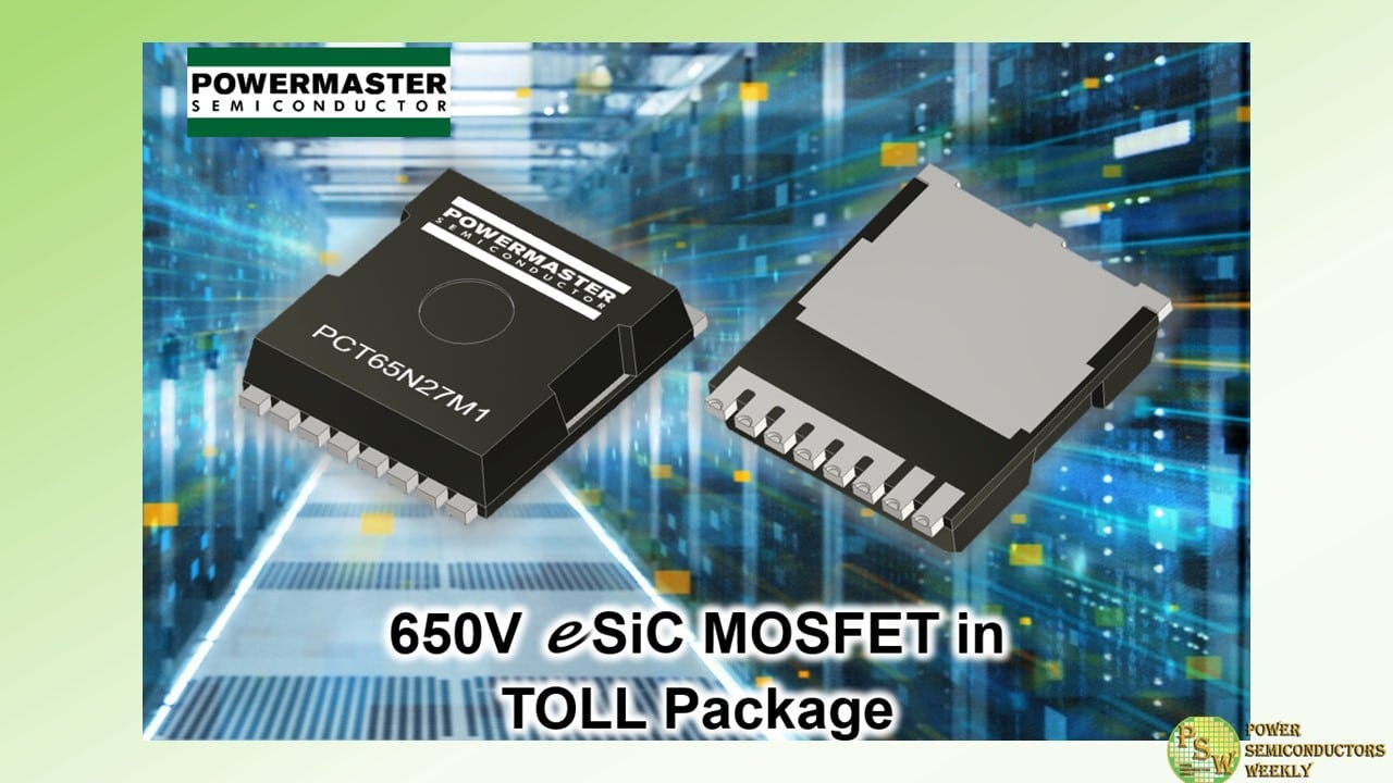
Power Master Semiconductor has released a new package portfolio, TO leadless (TOLL) package for 650V eSiC MOSFET series to meet the increasing demands for high power density and efficiency with superior switching performance in various applications such as AI data center servers, telecom infrastructure, flat panel display power, ESS, and battery formations.
Recently, the rapid growth of artificial intelligence (AI) is expected to drive continued strong data center demand. AI datacenters rely on GPUs that consume 10 to 15 times more power than traditional CPUs. SiC MOSFETs in TOLL package are an optimal solution for the rapidly expanding AI applications today.
The TOLL package has a footprint of 9.9mm x 11.7mm, reducing the PCB area by 30% compared to the D2PAK 7-lead package. Moreover, with a thickness of 2.3mm, it has 60% less height than the D2PAK 7-lead package.
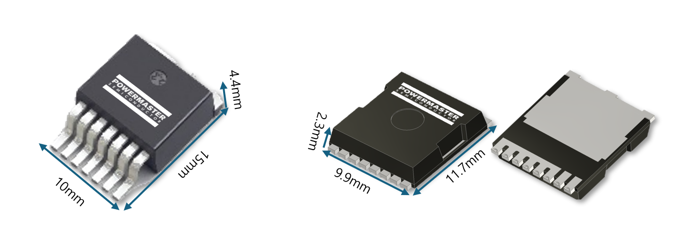
The TOLL offers superior thermal performance and low package inductance (2nH) compared to D2PAK 7-lead package. Kelvin source configuration lowers gate noise and reduces turn-on loss by 60% compared to same device without Kelvin source configuration, enabling higher frequency operation and improved power density. The new PCT65N27M1 has a VDSS rating of 650 V with a typical RDS(ON) of 27mΩ and a maximum drain current (ID) of 84 A.
Power Master Semiconductor’s products in TOLL package has special grooves in the gate and source pins to enhance the performance of the solder joint and offers Moisture Sensitivity Level 1 (MSL 1).
Original – Power Master Semiconductor
-
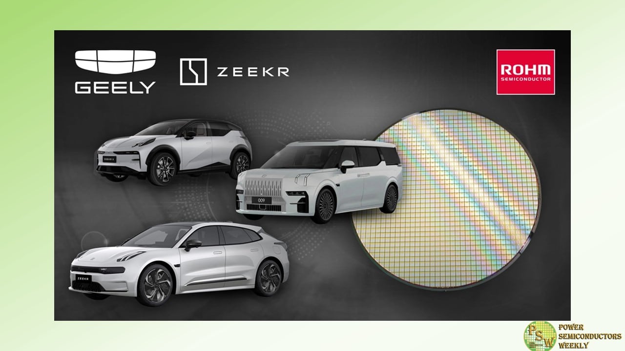
ROHM announced the adoption of power modules equipped with 4th generation SiC MOSFET bare chips for the traction inverters in three models of ZEEKR EV brand from Zhejiang Geely Holding Group (Geely), a top 10 global automaker. Since 2023, these power modules have been mass produced and shipped from HAIMOSIC (SHANGHAI) Co., Ltd. – a joint venture between ROHM and Zhenghai Group Co., Ltd. to Viridi E-Mobility Technology (Ningbo) Co., Ltd, a Tier 1 manufacturer under Geely.
Geely and ROHM have been collaborating since 2018, beginning with technical exchanges, then later forming a strategic partnership focused on SiC power devices in 2021. This led to the integration of ROHM’s SiC MOSFETs into the traction inverters of three models: the ZEEKR X, 009, and 001. In each of these EVs, ROHM’s power solutions centered on SiC MOSFETs play a key role in extending the cruising range and enhancing overall performance.
ROHM is committed to advancing SiC technology, with plans to launch 5th generation SiC MOSFETs in 2025 while accelerating market introduction of 6th and 7th generation devices. What’s more, by offering SiC in various forms, including bare chips, discrete components, and modules, ROHM is able to promote the widespread adoption of SiC technology, contributing to the creation of a sustainable society.
Original – ROHM
-

onsemi released the newest generation silicon and silicon carbide hybrid Power Integrated Modules (PIMs) in an F5BP package, ideally suited to boost the power output of utility-scale solar string inverters or energy storage system (ESS) applications. Compared to previous generations, the modules offer increased power density and higher efficiencies within the same footprint to increase the total system power of a solar inverter from 300kW up to 350kW.
This means a one-gigawatt (GW) capacity utility-scale solar farm using the latest generation modules can achieve an energy savings of nearly two megawatts (MW) per hour or the equivalent of powering more than 700 homes per year. Additionally, fewer modules are required to achieve the same power threshold as the previous generation, which can reduce power device component costs by more than 25%.
With solar power having achieved the lowest levelized cost of energy (LCOE), it is increasingly becoming the go-to source for renewable power generation around the world. To compensate for solar power’s variability, utility operators are also adding large-scale battery energy storage systems (BESS) to ensure a stable energy flow to the grid. To support this combination of systems, manufacturers and utilities require solutions that offer maximum efficiency and reliable power conversion. Every 0.1% of efficiency improvement can equate to a quarter of a million dollars in annual operational savings for every one gigawatt of installed capacity.
“As a variable energy source dependent on sunlight, continual advances in increasing system efficiencies, reliability and advanced storage solutions are needed to be able to maintain the stability and reliability of global grids during peak and off-peak power demand,” said Sravan Vanaparthy, vice president, Industrial Power Division, Power Solutions Group, onsemi. “A more efficient infrastructure increases adoption and assures us that, as more solar power generation is built out, less energy is wasted and pushes us forward on a path away from fossil fuels.”
The F5BP-PIMs are integrated with 1050V FS7 IGBT and the 1200V D3 EliteSiC diode to form a foundation that facilitates high voltage and high current power conversion while reducing power dissipation and increasing reliability. The FS7 IGBTs offer low turn-off losses and reduce switching losses by up to 8%, while the EliteSiC diodes provide superior switching performance and lower voltage flicker by 15% compared to previous generations.
These PIMs employ an innovative I-type Neutral Point Clamp (INPC) for the inverter module and a flying capacitor topology for the boost module. The modules also use an optimized electrical layout and advanced Direct Bonded Copper (DBC) substrates to reduce stray inductance and thermal resistance. In addition, a copper baseplate further decreases thermal resistance to the heat sink by 9.3%, ensuring the module remains cool under high operational loads. This thermal management is crucial in maintaining the efficiency and longevity of the modules, making them highly effective for demanding applications that require reliable and sustained power delivery.
Original – onsemi
