-
LATEST NEWS / PRODUCT & TECHNOLOGY / Si2 Min Read
WeEn Semiconductors announced an expansion to its range of high-performance and rugged IGBTs. Offering voltage ratings of 650V and 1200V, the new devices incorporate a fast recovery anti-parallel diode and boast extremely low leakage currents and exceptional conduction and switching characteristics at both high and low junction temperatures.
Based on an advanced fine trench gate field-stop (FS) technology, the new IGBTs provide a more uniform electric field within the chip, support higher breakdown voltages and offer improved dynamic control. By offering the optimum trade-off between conduction and switching losses, as well as an enhanced EMI design, the devices will maximize efficiency in a wide variety of mid- to high-switching-frequency power conversion designs.
The new IGBTs offer ratings of 650V/75A, 1200V/40A and 1200V/75A and are supplied in TO247 or TO247-4L packages depending on the selected device. All of the devices will operate with a maximum junction temperature (Tj) of 175 °C and have undergone high-voltage H3TRB (high-humidity, high-temperature and high-voltage reverse bias) and 100%-biased HTRB (high-temperature reverse bias) tests up to this maximum.
Target applications for the new WeEn IGBTs include solar inverters, motor control systems, uninterruptible power supplies (UPS) and welding. A positive temperature coefficient simplifies parallel operation in applications where higher performance is required, while options for bare die, discrete and module product variants provide flexibility for a wide variety of target designs.
Original – WeEn Semiconductors
-
LATEST NEWS4 Min Read
WeEn Semiconductors will be exhibiting the company’s latest highly efficient, high-power density silicon carbide (SiC) technologies, automotive grade power devices and highly reliable IGBTs at PCIM Europe 2024 in Nuremberg from June 11-13, 2024.
Established in 1979, PCIM Europe serves as a premier platform for showcasing the latest advancements in power electronics technologies and applications. This year, in Hall 9, booth 538, under the theme of ‘Power Efficiency for a Cooler Planet,’ WeEn Semiconductors will exhibit its extensive range of high-voltage 1700V SiC power modules, SiC 1200V/750V MOSFETs, Thyristors, power diodes, silicon-controlled rectifiers (SCRs), IGBTs, and other advanced power devices tailored for the renewable energy and e-mobility industries.
With a focus on efficiency, sustainability and cost reduction, WeEn’s broad portfolio offers best-in-class performance, efficiency and density for demanding applications including solar and wind power storage, electric vehicle (EV) fast chargers and traction inverters, HVAC and datacenter servers.
“At WeEn, we are dedicated to developing cost-effective power control technologies that support high voltage ratings and efficient, high-performance operation,” remarked WeEn Semiconductors CEO, Markus Mosen. “We’re excited to showcase the solutions we’ve launched in recent months at PCIM, not least those technologies targeted at renewable energy and electric mobility applications that demonstrate our commitment to products that not only meet but exceed the unique demands of every application while contributing to environmental sustainability.”
PCIM 2024 highlights
- At PCIM, WeEn is set to introduce a range of SiC MOSFETs and SiC Schottky Barrier Diodes (SBDs) in TSPAK packages for EV charging, On Board Charger (OBC), PV inverters, and high power density PSU applications. The new MOSFETs are available in 650V, 750V, 1200V, and 1700V variants, with resistance ranging from 20mΩ to 150mΩ. The current range for the new SiC SBDs is 10 to 40A in 650V, 750V, and 1200V variants.
- A range of SiC power modules in half-bridge, four-pack, six-pack, dual booster, and NPC 3L topologies will also be on display. Target markets for these SiC modules include EV charging, energy storage systems, motor drivers, industrial power supply units (PSUs), test instruments, and PV inverters.
- 1700V SiC series and 1200V / 750V auto-grade SiC MOSFETs, which encompass a diverse range of packaging options and product configurations, including surface-mount device (SMD) discrete components and top-side cooling.
- Highly reliable thyristor/diode modules, suitable for mainstream industrial applications like UPS, Inverter, soft starter, with VDRM up to 1600V and IT(RMS) up to 250A . Thanks for its planar chip technology and state-of-art module manufacture capability, those modules can be in half-bridge, parallel or antiparallel or other customized topology, it has passed 1000 hours reliability test under JEDEC standard as well 100% Pb-Free for the highest level EU RoHS compliance.
- WeEn’s product platforms include Super Junction MOSFETs with breakdown voltage ranges of 600V, 650V, and 800V. Leveraging advanced 8-inch wafer technology, WeEn offers a wide range of trench MOSFETs with voltage ranges from 20V to 30V.
- With voltage ratings from 45V to 2000V, WeEn’s Power Diodes feature current ratings from 1A to 100A. The company’s product portfolio includes low VF Schottky rectifiers, standard diodes, and ultrafast recovery rectifiers.
- WeEn’s range of IGBTs boasts extremely low leakage currents and exceptional conduction and switching characteristics at both high and low junction temperatures. They have undergone high voltage H3TRB and 100%-biased HTRB tests with a maximum junction temperature of 175°C safely. These application-specific IGBTs have been tuned to match the precise needs of each application, including switching behaviors, conduction losses, short circuit capabilities, environmental ruggedness, and freewheeling diode characterization. The 1200V and 650V variant current products, including bare dies, discrete components, and PIMs, are offered to various end customers.
Original – WeEn Semiconductors
-
LATEST NEWS / PRODUCT & TECHNOLOGY5 Min Read
As the “heart” of charging stations, the performance and reliability of charging modules are undeniably crucial. The popularization of the “super charging” concept has made long cruising range and short charging time become the selling points of more and more electric vehicles on the market.
Recently, the newly released Chinese Standard GB/T20234-2023, which focuses on Part 4: High-Power DC Charging Interfaces for Electric Vehicle Conductive Charging Couplers, has been significantly revised to expand the voltage range to 1500Vdc and the corresponding current range to 1000A. Additionally, the standard now includes new provisions related to liquid-cooled charging stations.
This means that in the future, higher-power megawatt-level charging stations will gradually become a reality. As long as your electric vehicle supports supercharging, it will be as convenient as refueling at a gas station.
Charging Module Technology Analysis
In fact, WeEn Semiconductors has long focused its business on the “low-carbon” track, while acknowledging that charging stations, as crucial supporting infrastructure, will evolve towards directions of higher power, greater efficiency, full liquid cooling, and comprehensive supercharging capabilities.
WeEn’s latest research and development effort, the BYC100MW-600PT2, will enable customers to achieve designs for 40kW+ high-power, high-efficiency charging modules. The WND60P20W will offer customers a higher voltage design margin to meet the demands of more complex and challenging application scenarios, thereby supporting the rapid development of new energy vehicles and the achievement of low-carbon objectives.
A charging module is essentially a power electronics converter that converts alternating current (AC) from power grid into direct current (DC) that can be stored in the battery of an electric vehicle.
Charging module converters typically have a two-stage topology. The first stage is usually a three-phase Power Factor Correction (PFC), most often using the Vienna PFC topology. Its main function is to convert AC to DC and to correct the power factor.
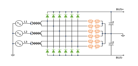
Figure 1: Vienna PFC Topology Architecture
The second stage typically involves a DC-DC conversion, most often using the high-efficiency LLC topology. This stage primarily converts the high voltage DC output from the PFC (800Vdc) into a wide range of adjustable DC voltages from 200Vdc to 1000Vdc, to match the needs of different battery voltage levels. Additionally, the DC-DC stage also achieves electrical isolation from the power grid through a high-frequency transformer.
Since the current charging modules are primarily used for delivering power to electric vehicles, the output rectification in the DC-DC stage commonly employs Fast Recovery Diodes (FRD). Benefiting from the negative temperature coefficient characteristics of Fast Recovery Diodes (FRD), and given that the LLC topology generally does not require stringent reverse recovery performance, FRDs are particularly suitable for use in charging modules that operate under high temperature and high current conditions.
Benefiting from the negative temperature coefficient characteristics of Fast Recovery Diodes (FRD), and given that the LLC topology generally does not require stringent reverse recovery performance, FRDs are particularly suitable for use in charging modules that operate under high temperature and high current conditions.
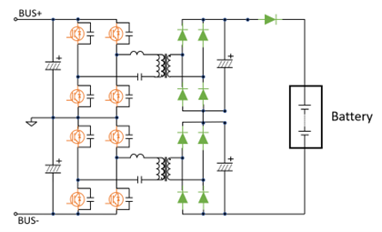
Figure 2: LLC DC- DC Topology Architecture
Currently, the mainstream power ratings for charging modules on the market range from 20kW to 40kW. Superchargers typically operate by outputting through several charging modules connected in parallel. Therefore, to ensure that each module is not affected by others during startup, Oring diodes are essential. When functioning normally, these diodes are in a conducting state, primarily incurring conduction losses. Consequently, standard rectifier diodes with low forward voltage (VF) are the best choice.
WeEn’s Professional Solutions
WeEn semiconductors, including the BYC75W-600P for LLC secondary-side rectification and the Oring diode WND60P16W, have been mass-produced reliably for years in leading charging module manufacturers’ 30kW models. With the recent trend towards higher power in charging modules and the need to accommodate for the harsh operating environments of charging stations, we have responded to our customers’ actual needs by launching the BYC100MW-600PT2 for 40kW charging modules and the higher voltage-resistant WND60P20W, helping our customers solve practical application issues.
#BYC100MW-600PT2 Features:
- Maximum current up to 100A
- Extremely low reverse leakage current
- Optimal VF-QRR trade-off performance
- Robust Eas capability
#WND60P20W Features:
- Maximum reverse voltage up to 2000 Vdc
- Extremely low forward conduction voltage drop
- Enhanced forward surge current capability
- Robust Eas capability
By comparing the specifications of the BYC100MW-600PT2 and BYC75W-600PT2, we find that the BYC100MW-600PT2 offers significant improvements in forward voltage (VF) while maintaining the same reverse recovery charge. As a result, it is more suitable for applications in 40kW high-power charging modules. Customers using the 40kW modules have observed an actual temperature rise reduction of 8°C to 10°C, which substantially enhances the thermal design of the system.
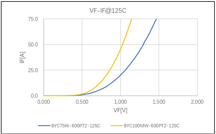
Figure 3: BYC100MW-600PT2 VF Curve
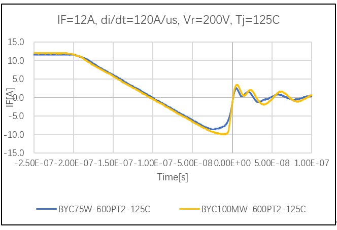
Figure 4: BYC100MW-600PT2 Qrr Curve
In the context of charging station applications, considering that there is quite a distance from the output of the charging module to the high-voltage power battery, potentially up to 30-40 meters, it is important to note that at the moment the charging module begins outputting, stray inductance in the charging cable and capacitors within the system will oscillate. This causes the diode to endure a spike in reverse voltage. If the voltage exceeds the diode’s avalanche voltage, it will cause avalanche breakdown; if the diode’s avalanche energy is insufficient, it will be damaged.
The WND60P20W is an enhancement of the existing WND60P16W product from WeEn Semiconductors, with the reverse withstand voltage increased to 2000Vdc while also improving its capability to withstand avalanche breakdown. The WND60P20W can meet the increasingly complex and harsh working environments of charging modules, providing greater safety margins for customer module designs.
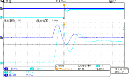
Figure 5: Voltage Oscillation Across Oring Diode
Original – WeEn Semiconductors
-
LATEST NEWS4 Min Read
It’s noteworthy that WeEn had already won the prestigious Haier COSMOPlat Excellent Supplier Award two years ago. Winning the supplier award again demonstrates WeEn’s leadership position in the market as an outstanding semiconductor supplier.
Both parties are excited about each other’s innovative potential as they promote closer collaboration, further signaling that WeEn will deepen and solidify its robust partnership with Haier COSMOPlat to accelerate the future of digital transformation across their industries.
Dating back to the former NXP era, Haier COSMOPlat has been an important ecosystem partner for WeEn. In today’s uncertain environment, while joyful outcomes may be hard to come by, having a strong technical foundation as support provides both companies with more cooperation opportunities.
As Haier COSMOPIat pursues trends of domestic resource localization and diversification, WeEn has stood out with its high quality and stringent quality control standards. Its products not only meet COSMOPIat’s high demands for stability and reliability, but also receive strong endorsement from COSMOPIat’s customers for partnering with high-quality domestic suppliers to drive coordinated development. This positions WeEn well to capitalize on opportunities for business growth.
Since 2020, global semiconductor supply chains have been impacted, but WeEn has remained proactive in addressing challenges of upstream supply shortages. By adjusting strategic deployments ahead of time and continuously supporting Haier COSMOPIat’s supply needs, WeEn has further strengthened the partnership between the two companies.
Last year, both parties signed a strategic cooperation agreement at the Hannover Messe in Germany, establishing a strategic partnership based on mutual assistance and win-win cooperation. These initiatives comprehensively facilitate Haier COSMOPIat’s digital transformation, accelerating the upgrade of end-to-end competitiveness. Simultaneously, they lay a solid foundation for future collaboration between the two companies in new technologies and market domains.
The continued development of Haier COSMOPIat has brought new opportunities and challenges for both parties, especially in the areas of digital transformation and ecosystem empowerment. The business leader of Haier COSMOPIat stated, “WeEn is a leading player among Chinese power semiconductor suppliers, with extensive technological expertise and a global presence. Its products are characterized by high quality, reliability, and cost-effectiveness. Thanks to WeEn’s unique position in the power semiconductor field, the range and diversity of products in the collaboration between the two parties continues to expand. The product line now spans from thyristors to power diodes, and further extends to TVS/ESD and silicon carbide product series. The level of cooperation is deepening continuously, showcasing the strong partnership between the two companies. In the future, we look forward to working hand in hand with WeEn to further explore the potential for cooperation and accelerate the digital transformation of the industry.”
Will Yin, Vice President of Global Sales & Marketing at WeEn, stated, “There is no doubt that digital transformation brings tremendous development potential to the power semiconductor industry.” WeEn looks forward to long-term cooperation with Haier COSMOPIat to embrace new opportunities and challenges brought by digitization, intelligence, and sustainability. Together, we will build diverse new development opportunities and jointly create new chapters of development in various fields. WeEn always stands at the forefront of industry development, leveraging a strong R&D and technical team to continuously strengthen the market sales and service team. This is to achieve steady growth in global business and contribute to industry transformation and innovation.
By the end of 2023, Haier COSMOPIat had established a new structure where the three business sectors of smart home controllers, diversified smart controllers across industries, and an industrial Internet platform in the electronics industry progressed simultaneously. COSMOPIat’s digital transformation has not only enhanced the agility of the supply chain but has also provided robust support for the industry’s digital transformation and upgrade through technological innovation and ecosystem empowerment.
In the future, WeEn will continue to focus on four major application areas: consumer electronics, renewable energy, big data, and automotive electronics. Leveraging its technological research and development strengths, WeEn will continue to expand investments in the power semiconductor field, actively increase production capacity, and grow together with its extensive customer base.
Original – WeEn Semiconductors


